JAJSHI4 May 2019 DRV8340-Q1
PRODUCTION DATA.
- 1 特長
- 2 アプリケーション
- 3 概要
- 4 改訂履歴
- 5 Device Comparison Table
- 6 Pin Configuration and Functions
- 7 Specifications
-
8 Detailed Description
- 8.1 Overview
- 8.2 Functional Block Diagram
- 8.3
Feature Description
- 8.3.1
Three Phase Smart Gate Drivers
- 8.3.1.1
PWM Control Modes
- 8.3.1.1.1 6x PWM Mode (PWM_MODE = 000b or MODE Pin Tied to AGND)
- 8.3.1.1.2 3x PWM Mode (PWM_MODE = 001b or MODE Pin = 18 kΩ to AGND)
- 8.3.1.1.3 1x PWM Mode (PWM_MODE = 010b or MODE Pin = 75 kΩ to AGND)
- 8.3.1.1.4 Independent Half-Bridge PWM Mode (PWM_MODE = 011b or MODE Pin is > 1.5 MΩ to AGND or Hi-Z)
- 8.3.1.1.5 Phases A and B are Independent Half-Bridges, Phase C is Independent FET (MODE = 100b)
- 8.3.1.1.6 Phases B and C are Independent Half-Bridges, Phase A is Independent FET (MODE = 101b or MODE Pin is 75 kΩ to DVDD)
- 8.3.1.1.7 Phases A is Independent Half-Bridge, Phases B and C are Independent FET (MODE = 110b or MODE Pin is 18 kΩ to DVDD)
- 8.3.1.1.8 Independent MOSFET Drive Mode (PWM_MODE = 111b or MODE Pin = 0.47 kΩ to DVDD)
- 8.3.1.2 Device Interface Modes
- 8.3.1.3 Gate Driver Voltage Supplies
- 8.3.1.4 Smart Gate Drive Architecture
- 8.3.1.1
PWM Control Modes
- 8.3.2 DVDD Linear Voltage Regulator
- 8.3.3 Pin Diagrams
- 8.3.4
Gate Driver Protective Circuits
- 8.3.4.1 VM Supply Undervoltage Lockout (UVLO)
- 8.3.4.2 VCP Charge Pump Undervoltage Lockout (CPUV)
- 8.3.4.3 MOSFET VDS Overcurrent Protection (VDS_OCP)
- 8.3.4.4 Gate Driver Fault (GDF)
- 8.3.4.5 Thermal Warning (OTW)
- 8.3.4.6 Thermal Shutdown (OTSD)
- 8.3.4.7 Open Load Detection (OLD)
- 8.3.4.8 Offline Shorts Diagnostics
- 8.3.4.9 Reverse Supply Protection
- 8.3.1
Three Phase Smart Gate Drivers
- 8.4 Device Functional Modes
- 8.5 Programming
- 8.6
Register Maps
- 8.6.1 Status Registers
- 8.6.2
Control Registers
- 8.6.2.1 IC1 Control Register (Address = 0x04) [reset = 0x00]
- 8.6.2.2 IC2 Control Register (address = 0x05) [reset = 0x40]
- 8.6.2.3 IC3 Control Register (Address = 0x06) [reset = 0xFF]
- 8.6.2.4 IC4 Control Register (Address = 0x07) [reset = 0xFF]
- 8.6.2.5 IC5 Control Register (Address = 0x08) [reset = 0xFF]
- 8.6.2.6 IC6 Control Register (Address = 0x09) [reset = 0x99]
- 8.6.2.7 IC7 Control Register (Address = 0x0A) [reset = 0x99]
- 8.6.2.8 IC8 Control Register (Address = 0x0B) [reset = 0x99]
- 8.6.2.9 IC9 Control Register (Address = 0x0C) [reset = 0x2F]
- 8.6.2.10 IC10 Control Register (Address = 0x0D) [reset = 0x61]
- 8.6.2.11 IC11 Control Register (Address = 0x0E) [reset = 0x00]
- 8.6.2.12 IC12 Control Register (Address = 0x0F) [reset = 0x2A]
- 8.6.2.13 IC13 Control Register (Address = 0x10) [reset = 0x7F]
- 8.6.2.14 IC14 Control Register (Address = 0x10) [reset = 0x00]
- 9 Application and Implementation
- 10Power Supply Recommendations
- 11Layout
- 12デバイスおよびドキュメントのサポート
- 13メカニカル、パッケージ、および注文情報
パッケージ・オプション
メカニカル・データ(パッケージ|ピン)
- PHP|48
サーマルパッド・メカニカル・データ
- PHP|48
発注情報
8.3.4.7.2 Open Load Detection in Active Mode (OLA)
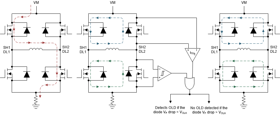
An open load in active mode is disabled by default in the SPI device and can be enabled independently per half-bridge by writing a 1 to the EN_OLA_x bit. In the H/W device, OLA runs if the nDIAG pin is left as unconnected or tied to GND. OLA is detected when the motor gets disconnected from the driver when it is commutating. Figure 30 shows a simplified H-bridge configuration for OLA implementation during high-side current recirculation. When the voltage drop across the body diode of the MOSFET does not exhibit overshoot greater than the VOLA over VM between the time the low-side FET is switched off and the high side FET is switched on during an output PWM cycle. An open load is not detected if the energy stored in the inductor is high enough to cause an overshoot greater than the VOLA over VM caused by the fly-back current flowing through the body diode of the high-side FET.
 Figure 30. Circuit for Open Load Detection in Active Mode
 NOTE
Depending on the operating conditions and on external circuitry, such as the output capacitors, an open load could be reported even though the load is present. This case might occur during a direction change or for small load currents respectively small PWM duty cycles. Therefore, TI recommends evaluating the open load diagnosis only in known suitable operating conditions and to ignore it otherwise.
The device has a failure counter to avoid inadvertent triggering of the open load active diagnosis. Three consecutive occurrences of the internal open load signal must occur, essentially three consecutive PWM pulses without freewheeling detected, before an open load is reported through the nFAULT pin and in the respective SPI register.
In the SPI device, depending on the load configuration and the PWM sequence, OLA on one phase can latch all three OL_PH_x bits high. In that case, the OLP diagnostic can be initiated to determine which phase has the open load condition. The load connections shown in Figure 29 are not supported by OLA.
For OLA to function correctly, place capacitors between the motor phase node and GND. This capacitor is required for BLDC, bi-directional BDC and unidirectional BDC motors at the phase node. If a solenoid load is connected, as shown in Figure 15, the capacitor is not required. Size the capacitors according Equation 3. Make sure that the capacitor (Cphase) is placed on the PCB.

where
- VTH is the threshold voltage of the MOSFET.
- VOLA(min) is 150 mV.
The values of Crss and Coss of the MOSFETs should be used for 0-V VDS. Derating of Cphase must be considered when selecting the capacitance.