JAJSCQ3E October 2016 – January 2021 DRV8702-Q1 , DRV8703-Q1
PRODUCTION DATA
- 1 特長
- 2 アプリケーション
- 3 概要
- 4 Revision History
- 5 Pin Configuration and Functions
- 6 Specifications
-
7 Detailed Description
- 7.1 Overview
- 7.2 Functional Block Diagram
- 7.3
Feature Description
- 7.3.1 Bridge Control
- 7.3.2 MODE Pin
- 7.3.3 nFAULT Pin
- 7.3.4 Current Regulation
- 7.3.5 Amplifier Output (SO)
- 7.3.6 PWM Motor Gate Drivers
- 7.3.7 IDRIVE Pin (DRV8702-Q1 Only)
- 7.3.8 Dead Time
- 7.3.9 Propagation Delay
- 7.3.10 Overcurrent VDS Monitor
- 7.3.11 VDS Pin (DRV8702-Q1 Only)
- 7.3.12 Charge Pump
- 7.3.13 Gate Drive Clamp
- 7.3.14
Protection Circuits
- 7.3.14.1 VM Undervoltage Lockout (UVLO2)
- 7.3.14.2 Logic Undervoltage (UVLO1)
- 7.3.14.3 VCP Undervoltage Lockout (CPUV)
- 7.3.14.4 Overcurrent Protection (OCP)
- 7.3.14.5 Gate Driver Fault (GDF)
- 7.3.14.6 Thermal Shutdown (TSD)
- 7.3.14.7 Watchdog Fault (WDFLT, DRV8703-Q1 Only)
- 7.3.14.8 Reverse Supply Protection
- 7.3.15 Hardware Interface
- 7.4 Device Functional Modes
- 7.5 Programming
- 7.6 Register Maps
- 8 Application and Implementation
- 9 Power Supply Recommendations
- 10Layout
- 11Device and Documentation Support
- 12Mechanical, Packaging, and Orderable Information
パッケージ・オプション
デバイスごとのパッケージ図は、PDF版データシートをご参照ください。
メカニカル・データ(パッケージ|ピン)
- RHB|32
サーマルパッド・メカニカル・データ
発注情報
8.2.2.2 IDRIVE Configuration
The IDRIVE current is selected based on the gate charge of the FETs. The IDRIVE pin must be configured so that the FET gates are charged entirely during the t(DRIVE) time. If the selected IDRIVE current is too low for a given FET, then the FET may not turn on completely. TI recommends adjusting these values in-system with the required external FETs and motor to determine the best possible setting for any application.
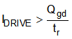
For FETs with a known gate-to-drain charge (Qgd) and desired rise time (tr), the IDRIVE current can be selected based on the Equation 6.
If the gate-to-drain charge is 2.3 nC and the desired rise time is around 100 to 300 ns, use Equation 7 to calculate the minimum IDRIVE (IDRIVE1) and Equation 8 to calculate the maximum IDRIVE (IDRIVE2).
Select a value for IDRIVE between 28 and 84 mA. An IDRIVE value of approximately 50 mA for the source (approximately 100 mA sink) was selected for this application. This value requires a 200-kΩ resistor from the IDRIVE pin to ground.