JAJSCQ3E October 2016 – January 2021 DRV8702-Q1 , DRV8703-Q1
PRODUCTION DATA
- 1 特長
- 2 アプリケーション
- 3 概要
- 4 Revision History
- 5 Pin Configuration and Functions
- 6 Specifications
-
7 Detailed Description
- 7.1 Overview
- 7.2 Functional Block Diagram
- 7.3
Feature Description
- 7.3.1 Bridge Control
- 7.3.2 MODE Pin
- 7.3.3 nFAULT Pin
- 7.3.4 Current Regulation
- 7.3.5 Amplifier Output (SO)
- 7.3.6 PWM Motor Gate Drivers
- 7.3.7 IDRIVE Pin (DRV8702-Q1 Only)
- 7.3.8 Dead Time
- 7.3.9 Propagation Delay
- 7.3.10 Overcurrent VDS Monitor
- 7.3.11 VDS Pin (DRV8702-Q1 Only)
- 7.3.12 Charge Pump
- 7.3.13 Gate Drive Clamp
- 7.3.14
Protection Circuits
- 7.3.14.1 VM Undervoltage Lockout (UVLO2)
- 7.3.14.2 Logic Undervoltage (UVLO1)
- 7.3.14.3 VCP Undervoltage Lockout (CPUV)
- 7.3.14.4 Overcurrent Protection (OCP)
- 7.3.14.5 Gate Driver Fault (GDF)
- 7.3.14.6 Thermal Shutdown (TSD)
- 7.3.14.7 Watchdog Fault (WDFLT, DRV8703-Q1 Only)
- 7.3.14.8 Reverse Supply Protection
- 7.3.15 Hardware Interface
- 7.4 Device Functional Modes
- 7.5 Programming
- 7.6 Register Maps
- 8 Application and Implementation
- 9 Power Supply Recommendations
- 10Layout
- 11Device and Documentation Support
- 12Mechanical, Packaging, and Orderable Information
パッケージ・オプション
デバイスごとのパッケージ図は、PDF版データシートをご参照ください。
メカニカル・データ(パッケージ|ピン)
- RHB|32
サーマルパッド・メカニカル・データ
発注情報
7.3.11 VDS Pin (DRV8702-Q1 Only)
The VDS pin on the DRV8702-Q1 device is used to select the VDS threshold voltage for overcurrent detection.
Tying the VDS pin to ground selects the lowest setting of 0.06 V. Leaving this pin open selects the setting of
0.48 V. Tying the VDS pin to the AVDD the pin disables the VDS monitor. For a detailed list of VDS configurations, see Table 7-8.
 Figure 7-14 VDS Block Diagram
Table 7-8 VDS Pin Resistor Setting
| VDS RESISTANCE | VDS VOLTAGE | OVERCURRENT TRIP LEVEL (VDS(OCP)) | CIRCUIT |
|---|---|---|---|
| < 1 kΩ to GND | GND | 0.06 V | 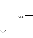 |
| 33 kΩ ± 5% to GND | 0.7 V ± 5% | 0.12 V | 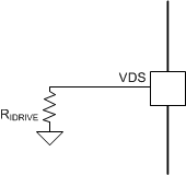 |
| 200 kΩ ± 5% to GND | 2 V ± 5% | 0.24 V | |
| > 2 MΩ to GND, Hi-Z | 3 V ± 5% | 0.48 V | 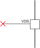 |
| 68 kΩ ± 5% to AVDD | 4 V ± 5% | 0.96 V | 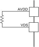 |
| < 1 kΩ to AVDD | AVDD | Disabled | 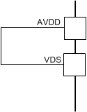 |