JAJSI41B February 2017 – October 2019 DS250DF210
PRODUCTION DATA.
- 1 特長
- 2 アプリケーション
- 3 概要
- 4 改訂履歴
- 5 概要(続き)
- 6 Pin Configuration and Functions
-
7 Specifications
- 7.1 Absolute Maximum Ratings
- 7.2 ESD Ratings
- 7.3 Recommended Operating Conditions
- 7.4 Thermal Information
- 7.5 Electrical Characteristics
- 7.6 Timing Requirements, Retimer Jitter Specifications
- 7.7 Timing Requirements, Retimer Specifications
- 7.8 Timing Requirements, Recommended Calibration Clock Specifications
- 7.9 Recommended SMBus Switching Characteristics (Slave Mode)
- 7.10 Recommended SMBus Switching Characteristics (Master Mode)
- 7.11 Typical Characteristics
-
8 Detailed Description
- 8.1 Overview
- 8.2 Functional Block Diagram
- 8.3
Feature Description
- 8.3.1 Device Data Path Operation
- 8.3.2 Signal Detect
- 8.3.3 Continuous Time Linear Equalizer (CTLE)
- 8.3.4 Variable Gain Amplifier (VGA)
- 8.3.5 Cross-Point Switch
- 8.3.6 Decision Feedback Equalizer (DFE)
- 8.3.7 Clock and Data Recovery (CDR)
- 8.3.8 Calibration Clock
- 8.3.9 Differential Driver With FIR Filter
- 8.3.10 Debug Features
- 8.3.11 Interrupt Signals
- 8.4 Device Functional Modes
- 8.5 Programming
- 8.6 Register Maps
- 9 Application and Implementation
- 10Power Supply Recommendations
- 11Layout
- 12デバイスおよびドキュメントのサポート
- 13メカニカル、パッケージ、および注文情報
9.2.1 Front-Port Jitter Cleaning Applications
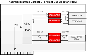
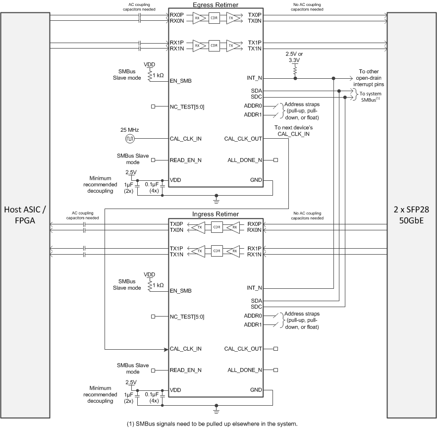
The DS250DF210 has strong equalization capabilities that allow it to equalize insertion loss, reduce jitter, and extend the reach of front-port interfaces. A single DS250DF210 can be used to support the egress and ingress channel of a 25GbE port. Similarly, two DS250DF210 devices can be used to support a 50GbE (2x25G) port, one DS250DF210 for the two egress channels and another DS250DF210 for the two ingress channels.
For applications which require IEEE802.3 100GBASE-CR4 or 25GBASE-CR auto-negotiation and link training, a linear repeater device such as the DS280BR810 (or similar) is recommended.
Figure 16 illustrates this configuration, and Figure 17 shows an example simplified schematic for a typical front-port application.
 Figure 16. Front-Port Application Block Diagram
  Figure 17. Front-Port Application Schematic