JAJSI56B September   2016  – October 2019 DS280BR820

PRODUCTION DATA.  

  1. 特長
  2. アプリケーション
  3. 概要
    1.     概略回路図
  4. 改訂履歴
  5. Pin Configuration and Functions
    1.     Pin Functions
  6. Specifications
    1. 6.1 Absolute Maximum Ratings
    2. 6.2 ESD Ratings
    3. 6.3 Recommended Operating Conditions
    4. 6.4 Thermal Information
    5. 6.5 Electrical Characteristics
    6. 6.6 Electrical Characteristics – Serial Management Bus Interface
    7. 6.7 Timing Requirements – Serial Management Bus Interface
    8. 6.8 Typical Characteristics
  7. Detailed Description
    1. 7.1 Overview
    2. 7.2 Functional Block Diagram
    3. 7.3 Feature Description
      1. 7.3.1 Device Data Path Operation
      2. 7.3.2 AC-Coupled Receiver Inputs
      3. 7.3.3 Signal Detect
      4. 7.3.4 2-Stage CTLE
      5. 7.3.5 Driver DC Gain Control
      6. 7.3.6 FIR Filter (Limiting Mode)
      7. 7.3.7 Configurable SMBus Address
    4. 7.4 Device Functional Modes
      1. 7.4.1 SMBus Slave Mode Configuration
      2. 7.4.2 SMBus Master Mode Configuration (EEPROM Self Load)
    5. 7.5 Programming
      1. 7.5.1 Transfer of Data with the SMBus Interface
    6. 7.6 Register Maps
      1. 7.6.1 Register Types: Global, Shared, and Channel
      2. 7.6.2 Global Registers: Channel Selection and ID Information
        1. Table 2. Global Register Map
      3. 7.6.3 Shared Registers
        1. Table 3. Shared Register Map
      4. 7.6.4 Channel Registers
        1. Table 4. Channel Register Map
  8. Application and Implementation
    1. 8.1 Application Information
    2. 8.2 Typical Applications
      1. 8.2.1 Backplane and Mid-Plane Reach Extension
        1. 8.2.1.1 Design Requirements
        2. 8.2.1.2 Detailed Design Procedure
      2. 8.2.2 Front-Port Applications
        1. 8.2.2.1 Design Requirements
        2. 8.2.2.2 Detailed Design Procedure
      3. 8.2.3 Application Curves
        1. 8.2.3.1 Pattern Generator Characteristics
        2. 8.2.3.2 Equalizing Moderate Pre-Channel Loss
        3. 8.2.3.3 Equalizing High Pre-Channel Loss
        4. 8.2.3.4 Equalizing High Pre-Channel Loss and Moderate Post-Channel Loss
        5. 8.2.3.5 Output in FIR Limiting Mode with 16T Pattern
    3. 8.3 Initialization Set Up
  9. Power Supply Recommendations
  10. 10Layout
    1. 10.1 Layout Guidelines
    2. 10.2 Layout Examples
      1. 10.2.1 Stripline Example
      2. 10.2.2 Microstrip Example
  11. 11デバイスおよびドキュメントのサポート
    1. 11.1 ドキュメントのサポート
      1. 11.1.1 関連資料
    2. 11.2 ドキュメントの更新通知を受け取る方法
    3. 11.3 商標
    4. 11.4 静電気放電に関する注意事項
    5. 11.5 Glossary

パッケージ・オプション

メカニカル・データ(パッケージ|ピン)
サーマルパッド・メカニカル・データ
発注情報

Stripline Example

The following example layout demonstrates how all signals can be escaped from the BGA array using stripline routing on a generic 8+ layer stackup. This example layout assumes the following:

  • Trace width: 0.15 mm (6 mil)
  • Trace edge-to-edge spacing: 0.16 mm (6.4 mil)
  • VIA finished hole size (diameter): 0.254 mm (10 mil)
  • VIA-to-VIA spacing: 1.0 mm (39 mil), to enhance PCB manufacturability
  • No VIA-in-pad used

Note that many other escape routing options exist using different trace width and spacing combinations. The optimum trace width and spacing will depend on the PCB material, PCB routing density, and other factors. Microstrip escape routing is also possible and may be preferable in some application scenarios such as front-port applications.
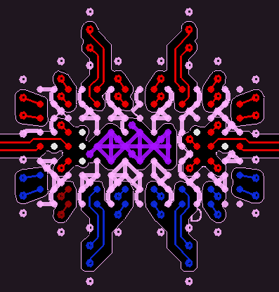
DS280BR820 top_left_top_layer_snls511.pngFigure 31. Stripline Example, Top Layer
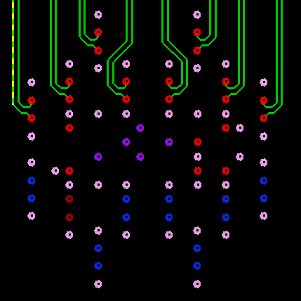
DS280BR820 bottom_left_internal_single_layer2_snls511.pngFigure 33. Stripline Example, Internal Signal Layer 2
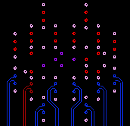
DS280BR820 top_right_internal_single_layer1_snls511.pngFigure 32. Stripline Example, Internal Signal Layer 1
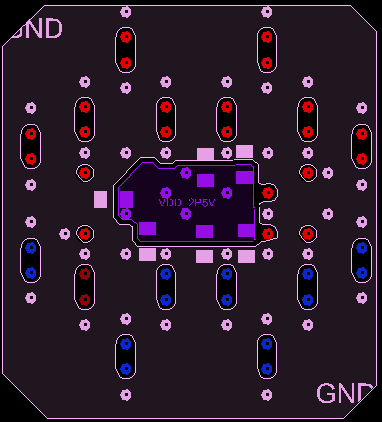
DS280BR820 bottom_layer_bottom_right_snls511.pngFigure 34. Stripline Example, Bottom Layer