SNLS302E May 2010 – February 2015 DS92LV2411 , DS92LV2412
PRODUCTION DATA.
- 1 Features
- 2 Applications
- 3 Description
- 4 Revision History
- 5 Pin Configuration and Functions
-
6 Specifications
- 6.1 Absolute Maximum Ratings
- 6.2 ESD Ratings
- 6.3 Recommended Operating Conditions
- 6.4 Thermal Information
- 6.5 Serializer DC Electrical Characteristics
- 6.6 Deserializer DC Electrical Characteristics
- 6.7 DC and AC Serial Control Bus Characteristics
- 6.8 Recommended Timing For The Serial Control Bus
- 6.9 Recommended Serializer Timing For CLKIN
- 6.10 Serializer Switching Characteristics
- 6.11 Deserializer Switching Characteristics
- 6.12 Typical Characteristics
-
7 Detailed Description
- 7.1 Overview
- 7.2 Functional Block Diagrams
- 7.3
Feature Description
- 7.3.1 Serializer Functional Description
- 7.3.2
Deserializer Functional Description
- 7.3.2.1 Integrated Signal Conditioning Features — Des
- 7.3.2.2 EMI Reduction Features
- 7.3.2.3 Power Saving Features
- 7.3.2.4 Des — Clock-Data Recovery Status Flag (Lock) And Output State Select (OSS_SEL)
- 7.3.2.5 Des — Oscillator Output — Optional
- 7.3.2.6 Des — OP_LOW — Optional
- 7.3.2.7 Des — Clock Edge Select (RFB)
- 7.3.2.8 Des — Control Signal Filter — Optional
- 7.3.2.9 Des — SSCG Low Frequency Optimization (Lf_mode)
- 7.3.2.10 Des — Strap Input Pins
- 7.3.3 Built In Self Test (BIST)
- 7.4 Device Functional Modes
- 7.5 Programming
- 7.6 Register Maps
- 8 Applications and Implementation
- 9 Power Supply Recommendations
- 10Layout
- 11Device and Documentation Support
- 12Mechanical, Packaging, and Orderable Information
7 Detailed Description
7.1 Overview
The DS92LV2411 / DS92LV2412 chipset transmits and receives 24-bits of data and 3 control signals over a single serial CML pair operating at 140 Mbps to 1.4 Gbps. The serial stream also contains an embedded clock, video control signals and the DC-balance information which enhances signal quality and supports AC coupling.
The Des can attain lock to a data stream without the use of a separate reference clock source, which greatly simplifies system complexity and overall cost. The Des also synchronizes to the Ser regardless of the data pattern, delivering true automatic “plug and lock” performance. It can lock to the incoming serial stream without the need of special training patterns or sync characters. The Des recovers the clock and data by extracting the embedded clock information, validating and then deserializing the incoming data stream providing a parallel LVCMOS video bus to the display or ASIC/FPGA.
The DS92LV2411 / DS92LV2412 chipset can operate in 24-bit color depth (with DE, HS, VS encoded within the serial data stream). In 18–bit color applications, the three video control signals maybe sent encoded within the serial bit stream (restrictions apply) along with six additional general purpose signals.
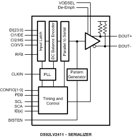
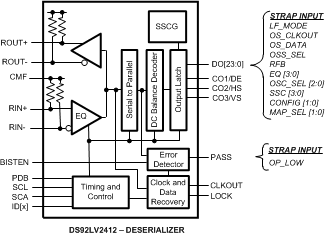
7.2 Functional Block Diagrams
7.3 Feature Description
7.3.1 Serializer Functional Description
The Ser converts a wide parallel input bus to a single serial output data stream, and also acts as a signal generator for the chipset Built In Self Test (BIST) mode. The device can be configured via external Pins or through the optional serial control bus. The Ser features enhance signal quality on the link by supporting: a selectable VOD level, a selectable de-emphasis signal conditioning and also the Channel Link II data coding that provides randomization, scrambling, and DC Balancing of the data. The Ser includes multiple features to reduce EMI associated with display data transmission. This includes the randomization and scrambling of the data and also the system spread spectrum clock support. The Ser features power saving features with a sleep mode, auto stop clock feature, and optional LVCMOS (1.8 V) parallel bus compatibility.
7.3.1.1 EMI Reduction Features
7.3.1.1.1 Data Randomization and Scrambling
Channel Link II Ser / Des feature a 3 step encoding process which enables the use of AC coupled interconnects and also helps to manage EMI. The serializer first passes the parallel data through a scrambler which randomizes the data. The randomized data is then DC balanced. The DC balanced and randomized data then goes through a bit shuffling circuit and is transmitted out on the serial line. This encoding process helps to prevent static data patterns on the serial stream. The resulting frequency content of the serial stream ranges from the parallel clock frequency to the nyquist rate. For example, if the Ser / Des chip set is operating at a parallel clock frequency of 50 MHz, the resulting frequency content of serial stream ranges from 50 MHz to 700 MHz ( 50 MHz *28 bits = 1.4 Gbps / 2 = 700 MHz ).
7.3.1.1.2 Ser — Spread Spectrum Compatibility
The Ser CLKIN is capable of tracking spread spectrum clocking (SSC) from a host source. The CLKIN will accept spread spectrum tracking up to 35 kHz modulation and ±0.5, ±1 or ±2% deviations (center spread). The maximum conditions for the CLKIN input are: a modulation frequency of 35 kHz and amplitude deviations of ±2% (4% total).
7.3.1.2 Integrated Signal Conditioning Features — Ser
7.3.1.2.1 Ser — VOD Select (VODSEL)
The Ser differential output voltage may be increased by setting the VODSEL Pin High. When VODSEL is Low, the VOD is at the standard (default) level. When VODSEL is High, the VOD is increased in level. The increased VOD is useful in extremely high noise environments and also on extra long cable length applications. When using de-emphasis it is recommended to set VODSEL = H to avoid excessive signal attenuation especially with the larger de-emphasis settings. This feature may be controlled by the external Pin or by register.
Table 1. Differential Output Voltage
| INPUT | EFFECT | |
|---|---|---|
| VODSEL | VOD mV |
VOD mVp-p |
| H | ±420 | 840 |
| L | ±280 | 560 |
7.3.1.2.2 Ser — De-Emphasis (De-Emph)
The De-Emph Pin controls the amount of de-emphasis beginning one full bit time after a logic transition that the Ser drives. This is useful to counteract loading effects of long or lossy cables. This Pin should be left open for standard switching currents (no de-emphasis) or if controlled by register. De-emphasis is selected by connecting a resistor on this Pin to ground, with R value between 0.5 kΩ to 1 MΩ, or by register setting. When using De-Emphasis it is recommended to set VODSEL = H.
Table 2. De-Emphasis Resistor Value
| RESISTOR VALUE (kΩ) | DE-EMPHASIS SETTING |
|---|---|
| Open | Disabled |
| 0.6 | - 12 dB |
| 1.0 | - 9 dB |
| 2.0 | - 6 dB |
| 5.0 | - 3 dB |
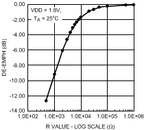 Figure 21. De-Emph vs. R Value
7.3.1.3 Power Saving Features
7.3.1.3.1 Ser — Power Down Feature (PDB)
The Ser has a PDB input Pin to ENABLE or POWER DOWN the device. This Pin is controlled by the host and is used to save power, disabling the link when the it is not needed. In the POWER DOWN mode, the high-speed driver outputs are both pulled to VDD and present a 0V VOD state. Note – in POWER DOWN, the optional Serial Bus Control Registers are RESET.
7.3.1.3.2 Ser — Stop Clock Feature
The Ser will enter a low power SLEEP state when the CLKIN is stopped. A STOP condition is detected when the input clock frequency is less than 3 MHz. The clock should be held at a static Low or high state. When the CLKIN starts again, the Ser will then lock to the valid input clock and then transmits the serial data to the Des. Note – in STOP CLOCK SLEEP, the optional Serial Bus Control Registers values are RETAINED.
7.3.1.3.3 1.8 V or 3.3 V VDDIO Operation
The Ser parallel bus and Serial Bus Interface can operate with 1.8 V or 3.3 V levels (VDDIO) for host compatibility. The 1.8 V levels will offer lower noise (EMI) and also a system power savings.
7.3.1.4 Ser — Pixel Clock Edge Select (RFB)
The RFB Pin determines the edge that the data is latched on. If RFB is High, input data is latched on the Rising edge of the CLKIN. If RFB is Low, input data is latched on the Falling edge of the CLKIN. Ser and Des maybe set differently. This feature may be controlled by the external Pin or by register.
7.3.1.5 Optional Serial Bus Control
Please see the following section on the optional Serial Bus Control Interface.
7.3.1.6 Optional BIST Mode
Please see the following section on the chipset BIST mode for details.
7.3.2 Deserializer Functional Description
The Des converts a single input serial data stream to a wide parallel output bus, and also provides a signal check for the chipset Built In Self Test (BIST) mode. The device can be configured via external Pins and strap Pins or through the optional serial control bus. The Des features enhance signal quality on the link with an integrated equalizer on the serial input and Channel Link II data encoding which provides randomization, scrambling, and DC balancing of the data. The Des includes multiple features to reduce EMI associated with data transmission. This includes the randomization and scrambling of the data, the output spread spectrum clock generation (SSCG) support and output clock and data slew rate select. The Des features power saving features with a power down mode, and optional LVCMOS (1.8 V) interface compatibility.
7.3.2.1 Integrated Signal Conditioning Features — Des
7.3.2.1.1 Des — Input Equalizer Gain (Eq)
The Des can enable receiver input equalization of the serial stream to increase the eye opening to the Des input. Note this function cannot be seen at the RxIN+/- input but can be observed at the serial test port (ROUT+/-) enabled via the Serial Bus control registers. The equalization feature may be controlled by the external Pin or by register.
Table 3. Receiver Equalization Configuration
| INPUTS | EFFECT | |||
|---|---|---|---|---|
| EQ3 | EQ2 | EQ1 | EQ0 | |
| L | L | L | H | ~1.5 dB |
| L | L | H | H | ~3 dB |
| L | H | L | H | ~4.5 dB |
| L | H | H | H | ~6 dB |
| H | L | L | H | ~7.5 dB |
| H | L | H | H | ~9 dB |
| H | H | L | H | ~10.5 dB |
| H | H | H | H | ~12 dB |
| X | X | X | L | OFF* |
| * Default Setting is EQ = Off | ||||
7.3.2.2 EMI Reduction Features
7.3.2.2.1 Des — Output Slew Rate Select (OS_CLKOUT/OS_DATA)
The parallel data outputs and clock outputs of the deserializer feature selectable output slew rates. The slew rate of the CLKOUT Pin is controlled by the strap Pin or register OS_CLKOUT, while the data outputs (DO[23:0] and CO[3:1]) are controlled by the strap Pin or register OS_DATA. When OS_CLKOUT/DATA = HIGH, the maximum slew rate is selected. When the OS_CLKOUT/DATA = LOW, the minimum slew rate is selected. Use the higher slew rate when driving longer traces or a heavier capacitive load.
7.3.2.2.2 Des — Common Mode Filter Pin (CMF) — Optional
The Des provides access to the center tap of the internal termination. A capacitor may be placed on this Pin for additional common-mode filtering of the differential pair. This can be useful in high noise environments for additional noise rejection capability. A 4.7 µF capacitor may be connected to this Pin to Ground.
7.3.2.2.3 Des — SSCG Generation — Optional
The Des provides an internally generated spread spectrum clock (SSCG) to modulate its outputs. Both clock and data outputs are modulated. This will aid to lower system EMI. Output SSCG deviations to ±2% (4% total) at up to 100 kHz modulations is available. See Table 4. This feature may be controlled by external STRAP Pins or by register.
Table 4. SSCG Configuration (LF_MODE = L) — Des Output
| SSC[3:0] INPUTS LF_MODE = L (20 - 50 MHz) |
RESULT | ||||
|---|---|---|---|---|---|
| SSC3 | SSC2 | SSC1 | SSC0 | fdev (%) | fmod (kHz) |
| L | L | L | L | NA | Disable |
| L | L | L | H | ±0.5 | CLK/2168 |
| L | L | H | L | ±1.0 | |
| L | L | H | H | ±1.5 | |
| L | H | L | L | ±2.0 | |
| L | H | L | H | ±0.5 | CLK/1300 |
| L | H | H | L | ±1.0 | |
| L | H | H | H | ±1.5 | |
| H | L | L | L | ±2.0 | |
| H | L | L | H | ±0.5 | CLK/868 |
| H | L | H | L | ±1.0 | |
| H | L | H | H | ±1.5 | |
| H | H | L | L | ±2.0 | |
| H | H | L | H | ±0.5 | CLK/650 |
| H | H | H | L | ±1.0 | |
| H | H | H | H | ±1.5 | |
Table 5. SSCG Configuration (Lf_mode = H) — Des Output
| SSC[3:0] INPUTS LH_MODE = H (5 - 20 MHz) |
RESULT | ||||
|---|---|---|---|---|---|
| SSC3 | SSC2 | SSC1 | SSC0 | fdev (%) | fmod (kHz) |
| L | L | L | L | NA | Disable |
| L | L | L | H | ±0.5 | CLK/620 |
| L | L | H | L | ±1.0 | |
| L | L | H | H | ±1.5 | |
| L | H | L | L | ±2.0 | |
| L | H | L | H | ±0.5 | CLK/370 |
| L | H | H | L | ±1.0 | |
| L | H | H | H | ±1.5 | |
| H | L | L | L | ±2.0 | |
| H | L | L | H | ±0.5 | CLK/258 |
| H | L | H | L | ±1.0 | |
| H | L | H | H | ±1.5 | |
| H | H | L | L | ±2.0 | |
| H | H | L | H | ±0.5 | CLK/192 |
| H | H | H | L | ±1.0 | |
| H | H | H | H | ±1.5 | |
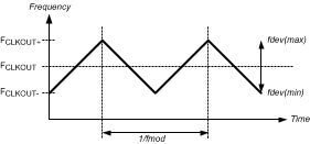 Figure 22. SSCG Waveform
7.3.2.2.4 1.8 V or 3.3 V VDDIO Operation
The Des parallel bus and Serial Bus Interface can operate with 1.8 V or 3.3 V levels (VDDIO) for target host compatibility. The 1.8 V levels will offer a lower noise (EMI) and also a system power savings.
7.3.2.3 Power Saving Features
7.3.2.3.1 Des — Powerdown Feature (PDB)
The Des has a PDB input Pin to ENABLE or POWER DOWN the device. This Pin can be controlled by the system to save power, disabling the Des when the display is not needed. An auto detect mode is also available. In this mode, the PDB Pin is tied High and the Des will enter POWER DOWN when the serial stream stops. When the serial stream starts up again, the Des will lock to the input stream and assert the LOCK Pin and output valid data. In POWER DOWN mode, the Data and CLKOUT output states are determined by the OSS_SEL status. Note – in POWER DOWN, the optional Serial Bus Control Registers are RESET.
7.3.2.3.2 Des — Stop Stream Sleep Feature
The Des will enter a low power SLEEP state when the input serial stream is stopped. A STOP condition is detected when the embedded clock bits are not present. When the serial stream starts again, the Des will then lock to the incoming signal and recover the data. Note – in STOP STREAM SLEEP, the optional Serial Bus Control Registers values are RETAINED.
7.3.2.4 Des — Clock-Data Recovery Status Flag (Lock) And Output State Select (OSS_SEL)
When PDB is driven HIGH, the CDR PLL begins locking to the serial input and LOCK goes from TRI-STATE to LOW (depending on the value of the OSS_SEL setting). After the DS92LV2412 completes its lock sequence to the input serial data, the LOCK output is driven HIGH, indicating valid data and clock recovered from the serial input is available on the parallel bus and clock outputs. The CLKOUT output is held at its current state at the change from OSC_CLK (if this is enabled via OSC_SEL) to the recovered clock (or vice versa).
If there is a loss of clock from the input serial stream, LOCK is driven Low and the state of the outputs are based on the OSS_SEL setting (STRAP Pin configuration or register).
7.3.2.5 Des — Oscillator Output — Optional
The Des provides an optional clock output when the input clock (serial stream) has been lost. This is based on an internal oscillator. The frequency of the oscillator may be selected. This feature may be controlled by the external Pin or by register. See Table 7 and Table 8.
Table 6. OSS_SEL And PDB Configuration — Des Outputs
| INPUTS | OUTPUTS | |||||
|---|---|---|---|---|---|---|
| SERIAL INPUT |
PDB | OSS_SEL | CLKOUT | DO[23:0], CO1, CO2, CO3 | LOCK | PASS |
| X | L | L | Z | Z | Z | Z |
| X | L | H | Z | Z | Z | Z |
| Static | H | L | L | L | L | L |
| Static | H | H | Z | Z* | L | L |
| Active | H | X | Active | Active | H | H |
| *NOTE — If Pin is strapped HIGH the output will be pulled up | ||||||
Table 7. OSC (Oscillator) Mode — Des Output
| INPUTS | OUTPUTS | |||
|---|---|---|---|---|
| EMBEDDED CLK | CLKOUT | DO[23:0]/CO1/CO2/CO3 | LOCK | PASS |
| NOTE * | OSC Output |
L | L | H |
| Present | Toggling | Active | H | H |
| * NOTE — Absent and OSC_SEL ≠ 000 | ||||
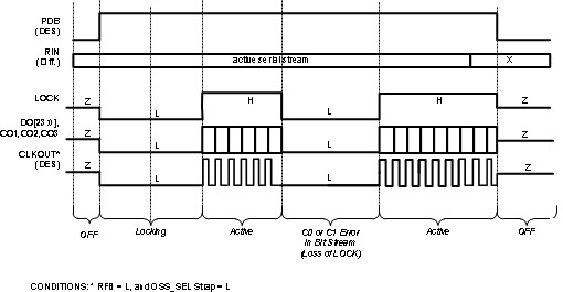 Figure 23. Des Outputs With Output State Select Low (OSS_SEL = L)
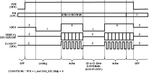 Figure 24. Des Outputs With Output State Select High (OSS_SEL = H)
Table 8. OSC_SEL (Oscillator) Configuration
| OSC_SEL[2:0] INPUTS | CLKOUT OSCILLATOR FREQUENCY | ||
|---|---|---|---|
| OSC_SEL2 | OSC_SEL1 | OSC_SEL0 | |
| L | L | L | Off – Feature Disabled – Default |
| L | L | H | 50 MHz ±40% |
| L | H | L | 25 MHz ±40% |
| L | H | H | 16.7 MHz ±40% |
| H | L | L | 12.5 MHz ±40% |
| H | L | H | 10 MHz ±40% |
| H | H | L | 8.3 MHz ±40% |
| H | H | H | 6.3 MHz ±40% |
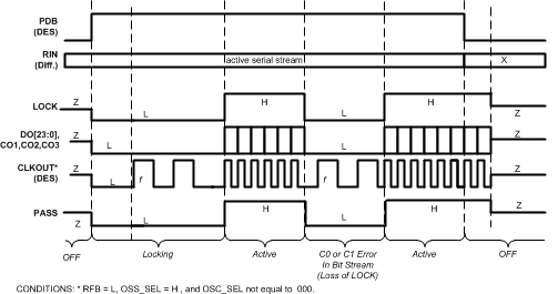 Figure 25. Des Outputs With Output State High And Clk Output Oscillator Option Enabled
7.3.2.6 Des — OP_LOW — Optional
The OP_LOW feature is used to hold the LVCMOS outputs, except for the LOCK output, at a LOW state. When the OP_LOW feature is enabled, the LVCMOS outputs will be held at logic LOW while LOCK = LOW. The user must toggle the OP_LOW Set/Reset register bit to release the outputs to the normal toggling state. Note that the release of the outputs can only occur when LOCK is HIGH. The OP_LOW strap option is assigned to the PASS Pin, at Pin location 42.
Restrictions on other straps:
- Other strap options should not be used in order to keep the data and clock outputs at a true logic LOW state. Other features should be selected through the I2C register interface.
- The OSS_SEL feature is not available when OP_LOW is enabled.
Outputs DO[23:0], CO[3:1] and CLKOUT are in TRI-STATE before PDB toggles HIGH because the OP-LOW strap value has not been recognized until the DS92LV2412 powers up. Figure 26 shows the user controlled release of the OP_LOW and automatic reset of OP_LOW set on the falling edge of LOCK. Figure 27 shows the user controlled release of OP_LOW and manual reset of OP_LOW set. Note manual reset of OP_LOW can only occur when LOCK is HIGH.
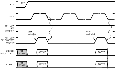 Figure 26. OP_LOW Auto Set
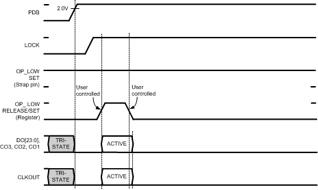 Figure 27. OP_LOW Manual Set/Reset
7.3.2.7 Des — Clock Edge Select (RFB)
The RFB Pin determines the edge that the data is strobed on. If RFB is High, output data is strobed on the Rising edge of the CLKOUT. If RFB is Low, data is strobed on the Falling edge of the CLKOUT. This allows for inter-operability with downstream devices. The Des output does not need to use the same edge as the Ser input. This feature may be controlled by the external Pin or by register.
7.3.2.8 Des — Control Signal Filter — Optional
The deserializer provides an optional Control Signal (C3, C2, C1) filter that monitors the three control signals and eliminates any pulses or glitches that are 1 or 2 parallel clock periods wide. Control signals must be 3 parallel clock periods wide (in its HIGH or LOW state, regardless of which state is active). This is set by the CONFIG[1:0] strap option or by I2C register control.
7.3.2.9 Des — SSCG Low Frequency Optimization (Lf_mode)
Text to come. This feature may be controlled by the external Pin or by Register.
7.3.2.10 Des — Strap Input Pins
Configuration of the device maybe done via configuration input Pins and the STRAP input Pins, or via the Serial Control Bus. The STRAP input Pins share select parallel bus output Pins. They are used to load in configuration values during the initial power up sequence of the device. Only a pull-up on the Pin is required when a HIGH is desired. By default the pad has an internal pull down, and will bias Low by itself. The recommended value of the pull up is 10 kΩ to VDDIO; open (NC) for Low, no pull-down is required (internal pull-down). If using the Serial Control Bus, no pull ups are required.
7.3.3 Built In Self Test (BIST)
An optional At-Speed Built In Self Test (BIST) feature supports the testing of the high-speed serial link. This is useful in the prototype stage, equipment production, in-system test and also for system diagnostics. In the BIST mode only a input clock is required along with control to the Ser and Des BISTEN input Pins. The Ser outputs a test pattern (PRBS7) and drives the link at speed. The Des detects the PRBS7 pattern and monitors it for errors. A PASS output Pin toggles to flag any payloads that are received with 1 to 24 errors. Upon completion of the test, the result of the test is held on the PASS output until reset (new BIST test or Power Down). A high on PASS indicates NO ERRORS were detected. A Low on PASS indicates one or more errors were detected. The duration of the test is controlled by the pulse width applied to the Des BISTEN Pin. During the BIST duration, the deserializer data outputs toggle with a checkerboard pattern.
Inter-operability is supported between this Channel Link II device and all Channel Link II generations (Gen 1/2/3).
Note: In order to use BIST mode, the BISTEN Pin must be pulled high and REG = 0. The serializer cannot be placed in BIST mode if REG = 1, as this will cause the DS92LV2411 to ignore the pin input voltage.
7.3.3.1 Sample BIST Sequence
See Figure 28 for the BIST mode flow diagram.
Step 1: Place the DS92LV2411 Ser in BIST Mode by setting Ser BISTEN = H. For the DS92LV2411 Ser or DS99R421 Channel Link II Ser BIST Mode is enabled via the BISTEN Pin. A CLKIN is required for BIST. When the Des detects the BIST mode pattern and command (DCA and DCB code) the data and control signal outputs are shut off.
Step 2: Place the DS92LV2412 Des in BIST mode by setting the BISTEN = H. The Des is now in the BIST mode and checks the incoming serial payloads for errors. If an error in the payload (1 to 24) is detected, the PASS Pin will switch low for one half of the clock period. During the BIST test, the PASS output can be monitored and counted to determine the payload error rate.
Step 3: To Stop the BIST mode, the Des BISTEN Pin is set Low. The Des stops checking the data and the final test result is held on the PASS Pin. If the test ran error free, the PASS output will be High. If there was one or more errors detected, the PASS output will be Low. The PASS output state is held until a new BIST is run, the device is RESET, or Powered Down. The BIST duration is user controlled by the duration of the BISTEN signal.
Step 4: To return the link to normal operation, the Ser BISTEN input is set Low. The Link returns to normal operation.
Figure 29 shows the waveform diagram of a typical BIST test for two cases. Case 1 is error free, and Case 2 shows one with multiple errors. In most cases it is difficult to generate errors due to the robustness of the link (differential data transmission etc.), thus they may be introduced by greatly extending the cable length, faulting the interconnect, reducing signal condition enhancements (De-Emphasis, VODSEL, or Rx Equalization).
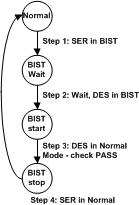 Figure 28. BIST Mode Flow Diagram
7.3.3.2 BER Calculations
It is possible to calculate the approximate Bit Error Rate (BER). The following is required:
- Clock Frequency (MHz)
- BIST Duration (seconds)
- BIST test Result (PASS)
The BER is less than or equal to one over the product of 24 times the CLK rate times the test duration. If we assume a 50 MHz clock, a 10 minute (600 second) test, and a PASS, the BERT is ≤ 1.39 X 10E-12
The BIST mode runs a check on the data payload bits. The LOCK Pin also provides a link status. It the recovery of the C0 and C1 bits does not reconstruct the expected clock signal, the LOCK Pin will switch Low. The combination of the LOCK and At-Speed BIST PASS Pin provides a powerful tool for system evaluation and performance monitoring.
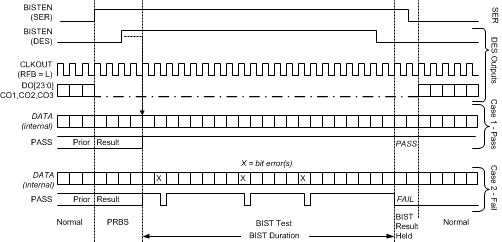 Figure 29. BIST Waveforms
7.4 Device Functional Modes
7.4.1 Data Transfer
The DS92LV2411 / DS92LV2412 chipset will transmit and receive a pixel of data in the following format: C1 and C0 represent the embedded clock in the serial stream. C1 is always HIGH and C0 is always LOW. The remaining 26 bit spaces contain the scrambled, encoded and DC-Balanced serial data.
7.4.2 Serializer and Deserializer Operating Modes and Reverse Compatibility (Config[1:0])
The DS92LV2411 / DS92LV2412 chipset is compatible with other single serial lane Channel Link II or FPD-Link II devices. Configuration modes are provided for reverse compatibility with the DS90C241 / DS90C124 and also the DS90UR241 / DS90UR124 by setting the respective mode with the CONFIG[1:0] Pins on the Ser or Des as shown in Table and Table. This selection also determines whether the Control Signal Filter feature is enabled or disabled in the Normal mode. These configuration modes are selectable the control Pins only.
Table 9. DS92LV2411 Serializer Modes
| CONFIG1 | CONFIG0 | MODE | DES DEVICE |
|---|---|---|---|
| L | L | Normal Mode, Control Signal Filter disabled | DS92LV2412, DS92LV2412, DS92LV0422, DS92LV0412 |
| L | H | Normal Mode, Control Signal Filter enabled | DS92LV2412, DS92LV2412, DS92LV0422, DS92LV0412 |
| H | L | Reverse Compatibility Mode | DS90UR124, DS99R124 |
| H | H | Reverse Compatibility Mode | DS90C124 |
Table 10. DS92LV2412 Serializer Modes
| CONFIG1 | CONFIG0 | MODE | SER DEVICE |
|---|---|---|---|
| L | L | Normal Mode, Control Signal Filter disabled | DS92LV2411, DS92LV2411, DS92LV0421, DS92LV0411 |
| L | H | Normal Mode, Control Signal Filter enabled | DS92LV2411, DS92LV2411, DS92LV0421, DS92LV0411 |
| H | L | Reverse Compatibility Mode | DS90UR241 |
| H | H | Reverse Compatibility Mode | DS90C241 |
7.4.3 Video Control Signal Filter — Serializer and Deserializer
When operating the devices in Normal Mode, the Control Signals have the following restrictions:
- Normal Mode with Control Signal Filter Enabled: Control Signal 1 and Control Signal 2 — Only 2 transitions per 130 clock cycles are transmitted, the transition pulse must be 3 parallel clocks or longer.
- Normal Mode with Control Signal Filter Disabled: Control Signal 1 and Control Signal 2 — Only 2 transitions per 130 clock cycles are transmitted, no restriction on minimum transition pulse.
- Control Signal 3 — Only 1 transition per 130 clock cycles is transmitted , minimum pulse width is 130 clock cycles.
Control Signals are defined as low frequency signals with limited transition. Glitches of a control signal can cause a visual error in display applications. This feature allows for the chipset to validate and filter out any high frequency noise on the control signals. See Figure.
7.5 Programming
7.5.1 Optional Serial Bus Control
The Ser and Des may also be configured by the use of a serial control bus that is I2C protocol compatible. By default, the I2C reg_0x00'h is set to 00'h and all configuration is set by control/strap Pins. A write of 01'h to reg_0x00'h will enable/allow configuration by registers; this will override the control/strap Pins. Multiple devices may share the serial control bus since multiple addresses are supported. See Figure 30.
The serial bus is comprised of three Pins. The SCL is a Serial Bus Clock Input. The SDA is the Serial Bus Data Input / Output signal. Both SCL and SDA signals require an external pull up resistor to VDDIO. For most applications a 4.7 k pull up resistor to VDDIO may be used. The resistor value may be adjusted for capacitive loading and data rate requirements. The signals are either pulled High, or driven Low.
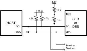 Figure 30. Serial Control Bus Connection
The third Pin is the ID[X] Pin. This Pin sets one of four possible device addresses. As shown in Figure 30 , Table 11 and Table 12 different Resistor values could be used to set different SMBUS addresses.
The Serial Bus protocol is controlled by START, START-Repeated, and STOP phases. A START occurs when SDA transitions Low while SCL is High. A STOP occurs when SDA transition High while SCL is also HIGH. See Figure 31
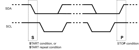 Figure 31. Start and Stop Conditions
To communicate with a remote device, the host controller (master) sends the slave address and listens for a response from the slave. This response is referred to as an acknowledge bit (ACK). If a slave on the bus is addressed correctly, it Acknowledges (ACKs) the master by driving the SDA bus low. If the address doesn't match a device's slave address, it Not-acknowledges (NACKs) the master by letting SDA be pulled High. ACKs also occur on the bus when data is being transmitted. When the master is writing data, the slave ACKs after every data byte is successfully received. When the master is reading data, the master ACKs after every data byte is received to let the slave know it wants to receive another data byte. When the master wants to stop reading, it NACKs after the last data byte and creates a stop condition on the bus. All communication on the bus begins with either a Start condition or a Repeated Start condition. All communication on the bus ends with a Stop condition. A READ is shown in Figure 32 and a WRITE is shown in Figure 33.
If the Serial Bus is not required, the three Pins may be left open (NC).
Table 11. Id[X] Resistor Value – DS92LV2411 Serializer
| RESISTOR RID kΩ |
ADDRESS 7'b |
ADDRESS 8'b 0 APPENDED (WRITE) |
|---|---|---|
| 0.47 | 7b' 110 1001 (h'69) | 8b' 1101 0010 (h'D2) |
| 2.7 | 7b' 110 1010 (h'6A) | 8b' 1101 0100 (h'D4) |
| 8.2 | 7b' 110 1011 (h'6B) | 8b' 1101 0110 (h'D6) |
| Open | 7b' 110 1110 (h'6E) | 8b' 1101 1100 (h'DC) |
Table 12. Id[X] Resistor Value – DS92LV2412 Deserializer
| RESISTOR RID kΩ |
ADDRESS 7'b |
ADDRESS 8'b 0 APPENDED (WRITE) |
|---|---|---|
| 0.47 | 7b' 111 0001 (h'71) | 8b' 1110 0010 (h'E2) |
| 2.7 | 7b' 111 0010 (h'72) | 8b' 1110 0100 (h'E4) |
| 8.2 | 7b' 111 0011 (h'73) | 8b' 1110 0110 (h'E6) |
| Open | 7b' 111 0110 (h'76) | 8b' 1110 1100 (h'EC) |
 Figure 32. Serial Control Bus — Read
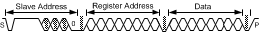 Figure 33. Serial Control Bus — Write
7.6 Register Maps
Table 13. Serializer — Serial Bus Control Registers
| ADD (dec) |
ADD (hex) |
REGISTER NAME |
Bit(s) | R/W | DEFAULT (bin) |
FUNCTION | DESCRIPTION |
|---|---|---|---|---|---|---|---|
| 0 | 0 | Ser Config 1 | 7 | R/W | 0 | Reserved | Reserved |
| 6 | R/W | 0 | Reserved | Reserved | |||
| 5 | R/W | 0 | VODSEL | 0: Low 1: High |
|||
| 4 | R/W | 0 | RFB | 0: Data latched on Falling edge of CLKIN 1: Data latched on Rising edge of CLKIN |
|||
| 3:2 | R/W | 00 | CONFIG | 00: Control Signal Filter Disabled 01: Control Signal Filter Enabled 10: Reserved 11: Reserved |
|||
| 1 | R/W | 0 | SLEEP | Note – not the same function as PowerDown (PDB) 0: normal mode 1: Sleep Mode – Register settings retained. |
|||
| 0 | R/W | 0 | REG | 0: Configurations set from control Pins 1: Configuration set from registers (except I2C_ID) |
|||
| 1 | 1 | Device ID | 7 | R/W | 0 | REG ID | 0: Address from ID[X] Pin 1: Address from Register |
| 6:0 | R/W | 1101000 | ID[X] | Serial Bus Device ID, Four IDs are: 7b '1101 001 (h'69) 7b '1101 010 (h'6A) 7b '1101 011 (h'6B) 7b '1101 110 (h'6E) All other addresses are Reserved. |
|||
| 2 | 2 | De-Emphasis Control | 7:5 | R/W | 000 | De-E Setting | 000: set by external Resistor 001: -1 dB 010: -2 dB 011: -3.3 dB 100: -5 dB 101: -6.7 dB 110: -9 dB 111: -12 dB |
| 4 | R/W | 0 | De-E EN | 0: De-Emphasis Enabled 1: De-Emphasis Disabled |
|||
| 3:0 | R/W | 000 | Reserved | Reserved |