SNLS302E May 2010 – February 2015 DS92LV2411 , DS92LV2412
PRODUCTION DATA.
- 1 Features
- 2 Applications
- 3 Description
- 4 Revision History
- 5 Pin Configuration and Functions
-
6 Specifications
- 6.1 Absolute Maximum Ratings
- 6.2 ESD Ratings
- 6.3 Recommended Operating Conditions
- 6.4 Thermal Information
- 6.5 Serializer DC Electrical Characteristics
- 6.6 Deserializer DC Electrical Characteristics
- 6.7 DC and AC Serial Control Bus Characteristics
- 6.8 Recommended Timing For The Serial Control Bus
- 6.9 Recommended Serializer Timing For CLKIN
- 6.10 Serializer Switching Characteristics
- 6.11 Deserializer Switching Characteristics
- 6.12 Typical Characteristics
-
7 Detailed Description
- 7.1 Overview
- 7.2 Functional Block Diagrams
- 7.3
Feature Description
- 7.3.1 Serializer Functional Description
- 7.3.2
Deserializer Functional Description
- 7.3.2.1 Integrated Signal Conditioning Features — Des
- 7.3.2.2 EMI Reduction Features
- 7.3.2.3 Power Saving Features
- 7.3.2.4 Des — Clock-Data Recovery Status Flag (Lock) And Output State Select (OSS_SEL)
- 7.3.2.5 Des — Oscillator Output — Optional
- 7.3.2.6 Des — OP_LOW — Optional
- 7.3.2.7 Des — Clock Edge Select (RFB)
- 7.3.2.8 Des — Control Signal Filter — Optional
- 7.3.2.9 Des — SSCG Low Frequency Optimization (Lf_mode)
- 7.3.2.10 Des — Strap Input Pins
- 7.3.3 Built In Self Test (BIST)
- 7.4 Device Functional Modes
- 7.5 Programming
- 7.6 Register Maps
- 8 Applications and Implementation
- 9 Power Supply Recommendations
- 10Layout
- 11Device and Documentation Support
- 12Mechanical, Packaging, and Orderable Information
6 Specifications
6.1 Absolute Maximum Ratings(12)(1)(1)
| MIN | MAX | UNIT | ||
|---|---|---|---|---|
| Supply Voltage – VDDn (1.8 V) | −0.3 | 2.5 | V | |
| Supply Voltage – VDDIO | −0.3 | 4.0 | V | |
| LVCMOS I/O Voltage | −0.3 | (VDDIO + 0.3) | V | |
| Receiver Input Voltage | −0.3 | (VDD + 0.3) | V | |
| Driver Output Voltage | −0.3 | (VDD + 0.3) | V | |
| Junction Temperature | +150 | °C | ||
| Storage Temperature Range (Tstg) | −65 | +150 | °C | |
(1) For soldering specifications, see product folder at www.ti.com and http://www.ti.com/lit/SNOA549
6.2 ESD Ratings
| VALUE | UNIT | |||
|---|---|---|---|---|
| V(ESD) | Electrostatic discharge | Human-body model (HBM), per ANSI/ESDA/JEDEC JS-001(1) | ±8000 | V |
| Charged-device model (CDM), per JEDEC specification JESD22-C101(2) | ±1000 | |||
| Machine Model (MM) | ±250 | |||
| IEC61000–4–2), RD = 330Ω, CS = 150pF | ||||
| V(ESD) | Electrostatic discharge | Air Discharge (DOUT+, DOUT-) | ±2500 | V |
| Contact Discharge (DOUT+, DOUT-) | ±800 | |||
| Air Discharge (RIN+, DIN-) | ±2500 | |||
| Contact Discharge (RIN+, RIN-) | ±800 | |||
(1) JEDEC document JEP155 states that 500-V HBM allows safe manufacturing with a standard ESD control process. Manufacturing with less than 500-V HBM is possible if necessary precautions are taken. Pins listed as DOUT+, DOUT- or RIN+, DIN- may actually have higher performance.
(2) JEDEC document JEP157 states that 250-V CDM allows safe manufacturing with a standard ESD control process. Manufacturing with less than 250-V CDM is possible if necessary precautions are taken. Pins listed as DOUT+, DOUT- or RIN+, DIN- may actually have higher performance.
6.3 Recommended Operating Conditions
| MIN | TYP | MAX | UNIT | |
|---|---|---|---|---|
| Supply Voltage (VDDn) | 1.71 | 1.8 | 1.89 | V |
| LVCMOS Supply Voltage (VDDIO) | 1.71 | 1.8 | 1.89 | V |
| OR | ||||
| LVCMOS Supply Voltage (VDDIO) | 3.0 | 3.3 | 3.6 | V |
| Operating Free Air Temperature (TA) | −40 | +25 | +85 | °C |
| Clock Frequency | 5 | 50 | MHz | |
| Supply Noise(10) | 50 | mVP-P |
6.4 Thermal Information
| THERMAL METRIC(1) | RHS(2) | NKB(3) | UNIT | |
|---|---|---|---|---|
| 48 PINS | 60 PINS | |||
| RθJA | Junction-to-ambient thermal resistance | 27.1 | 24.6 | °C/W |
| RθJC(top) | Junction-to-case (top) thermal resistance | 4.5 | 2.8 | |
(1) For more information about traditional and new thermal metrics, see the IC Package Thermal Metrics application report, SPRA953.
(2) Ratings for maximum dissipation capacity (215 mW).
(3) Ratings for maximum dissipation capacity (478 mW).
6.5 Serializer DC Electrical Characteristics
Over recommended operating supply and temperature ranges unless otherwise specified.(2)(3)(4)| PARAMETER | TEST CONDITIONS | PIN/FREQ. | MIN | TYP | MAX | UNIT | ||
|---|---|---|---|---|---|---|---|---|
| LVCMOS INPUT DC SPECIFICATIONS | ||||||||
| VIH | High Level Input Voltage | VDDIO = 3.0 to 3.6V | DI[23:0], CI1,CI2,CI3, CLKIN, PDB, VODSEL, RFB, BISTEN, CONFIG[1:0] | 2.2 | VDDIO | V | ||
| VDDIO = 1.71 to 1.89V | 0.65* VDDIO |
VDDIO | ||||||
| VIL | Low Level Input Voltage | VDDIO = 3.0 to 3.6V | GND | 0.8 | V | |||
| VDDIO = 1.71 to 1.89V | GND | 0.35* VDDIO |
||||||
| IIN | Input Current | VIN = 0V or VDDIO | VDDIO = 3.0 to 3.6V | –15 | ±1 | +15 | μA | |
| VDDIO = 1.71 to 1.89V | –15 | ±1 | +15 | |||||
| CML DRIVER DC SPECIFICATIONS | ||||||||
| VOD | Differential Output Voltage | RL = 100Ω, De-emph = disabled, Figure 2 | VODSEL = 0 | DOUT+, DOUT- | ±205 | ±280 | ±355 | mV |
| VODSEL = 1 | ±320 | ±420 | ±520 | |||||
| VODp-p | Differential Output Voltage (DOUT+) – (DOUT-) | VODSEL = 0 | 560 | mVp-p | ||||
| VODSEL = 1 | 840 | mVp-p | ||||||
| ΔVOD | RL = 100Ω, De-emph = disabled, VODSEL = L | 1 | 50 | mV | ||||
| VOS | Offset Voltage – Single-ended At TP A and B, Figure 1 | RL = 100Ω, De-emph = disabled | VODSEL = 0 | 0.65 | V | |||
| VODSEL = 1 | 1.575 | V | ||||||
| ΔVOS | Offset Voltage Unbalance Single-ended At TP A and B, Figure 1 | RL = 100Ω, De-emph = disabled | 1 | mV | ||||
| IOS | Output Short Circuit Current | DOUT+/- = 0V, De-emph = disabled | VODSEL = 0 | –36 | mA | |||
| RTO | Internal Output Termination Resistor | 80 | 100 | 120 | Ω | |||
| SUPPLY CURRENT | ||||||||
| IDDT1 | Serializer Supply Current (includes load current) RL = 100 Ω, CLKIN = 50 MHz | Checker Board Pattern, De-emph = 3kΩ, VODSEL = H, Figure 9 | VDD = 1.89V | All VDD Pins | 75 | 85 | mA | |
| VDDIO = 1.89V | VDDIO | 3 | 5 | mA | ||||
| IDDIOT1 | VDDIO = 3.6V | 11 | 15 | mA | ||||
| IDDT2 | Checker Board Pattern, De-emph = 6kΩ, VODSEL = L, Figure 9 | VDD33 = 1.89V | All VDD Pins | 65 | 75 | mA | ||
| VDDIO = 1.89V | VDDIO | 3 | 5 | mA | ||||
| IDDIOT2 | VDDIO = 3.6V | 11 | 15 | mA | ||||
| IDDZ | Serializer Supply Current Power-down | PDB = 0V , (All other LVCMOS Inputs = 0V) | VDD33 = 1.89V | All VDD Pins | 40 | 1000 | µA | |
| VDDIO = 1.89V | VDDIO | 5 | 10 | µA | ||||
| IDDIOZ | VDDIO = 3.6V | 10 | 20 | µA | ||||
6.6 Deserializer DC Electrical Characteristics
Over recommended operating supply and temperature ranges unless otherwise specified.(2)(3)(4)| PARAMETER | TEST CONDITIONS | PIN/FREQ. | MIN | TYP | MAX | UNIT | ||
|---|---|---|---|---|---|---|---|---|
| 3.3 V I/O LVCMOS DC SPECIFICATIONS – VDDIO = 3.0 to 3.6V | ||||||||
| VIH | High Level Input Voltage | PDB, BISTEN | 2.2 | VDDIO | V | |||
| VIL | Low Level Input Voltage | GND | 0.8 | V | ||||
| IIN | Input Current | VIN = 0V or VDDIO | –15 | ±1 | +15 | μA | ||
| VOH | High Level Output Voltage | IOH = −0.5 mA, RDS = L | DO[23:0], CO1, CO2, CO3, CLKOUT, LOCK, PASS | 2.4 | VDDIO | V | ||
| V | ||||||||
| VOL | Low Level Output Voltage | IOL = +0.5 mA, RDS = L | GND | 0.4 | V | |||
| IOS | Output Short Circuit Current | VDDIO = 3.3V, VOUT = 0V, OS_PCLK/DATA = L/H | CLKOUT | 36 | mA | |||
| VDDIO = 3.3V, VOUT = 0V, OS_PCLK/DATA = L/H | Outputs | |||||||
| IOZ | TRI-STATE Output Current | PDB = 0V, OSS_SEL = 0V, VOUT = H | Outputs | –15 | +15 | μA | ||
| 1.8 V I/O LVCMOS DC SPECIFICATIONS – VDDIO = 1.71 to 1.89V | ||||||||
| VIH | High Level Input Voltage | PDB, BISTEN | 1.235 | VDDIO | V | |||
| VIL | Low Level Input Voltage | GND | 0.595 | V | ||||
| IIN | Input Current | VIN = 0V or VDDIO | –15 | ±1 | +15 | µA | ||
| VOH | High Level Output Voltage | IOH = −0.5 mA, RDS = L | DO[23:0], CO1, CO2, CO3, CLKOUT, LOCK, PASS | VDDIO – 0.45 | VDDIO | V | ||
| VOL | Low Level Output Voltage | IOL = +0.5 mA, RDS = L | GND | 0.45 | V | |||
| IOS | Output Short Circuit Current | VDDIO = 1.8V, VOUT = 0V, OS_PCLK/DATA = L/H | CLKOUT | 18 | mA | |||
| VDDIO = 1.8V, VOUT = 0V, OS_PCLK/DATA = L/H | Outputs | 18 | mA | |||||
| IOZ | TRI-STATE Output Current | PDB = 0V, OSS_SEL = 0V, VOUT = H | Outputs | –15 | +15 | µA | ||
| CML RECEIVER DC SPECIFICATIONS | ||||||||
| VTH | Differential Input Threshold High Voltage | VCM = +1.2V (Internal VBIAS) | RIN+, RIN- | +50 | mV | |||
| VTL | Differential Input Threshold Low Voltage | –50 | mV | |||||
| VCM | Common Mode Voltage, Internal VBIAS | 12 | V | |||||
| IIN | Input Current | VIN = 0V or VDDIO | –15 | +15 | µA | |||
| RTI | Internal Input Termination Resistor | RIN+, RIN- | 80 | 100 | 120 | Ω | ||
| LOOP THROUGH CML DRIVER OUTPUT DC SPECIFICATIONS – EQ TEST PORT | ||||||||
| VOD | Differential Output Voltage | RL = 100Ω | ROUT+/- | 542 | mV | |||
| VOS | Offset Voltage Single-ended | RL = 100Ω | 1.4 | V | ||||
| RT | Internal Termination Resistor | ROUT+/- | 80 | 100 | 120 | Ω | ||
| SUPPLY CURRENT | ||||||||
| IDD1 | Deserializer Supply Current (includes load current) CLKOUT = 50 MHz |
Checker Board Pattern, RDS = H, CL = 4pF, Figure 9 |
VDD = 1.89V | All VDD Pins | 93 | 110 | mA | |
| VDDIO = 1.89V | VDDIO | 33 | 45 | mA | ||||
| IDDIO1 | VDDIO = 3.6V | 62 | 75 | mA | ||||
| IDDZ | Deserializer Supply Current Power Down | PDB = 0V, All other LVCMOS Inputs = 0V | VDD = 1.89V | All VDD Pins | 40 | 3000 | µA | |
| VDDIO = 1.89V | VDDIO | 5 | 50 | µA | ||||
| IDDIOZ | VDDIO = 3.6V | 10 | 100 | µA | ||||
6.7 DC and AC Serial Control Bus Characteristics
Over recommended operating supply and temperature ranges unless otherwise specified.| PARAMETER | TEST CONDITIONS | MIN | TYP | MAX | UNIT | |
|---|---|---|---|---|---|---|
| VIH | Input High Level | SDA and SCL | 2.2 | VDD 3.3V | V | |
| VIL | Input Low Level Voltage | SDA and SCL | GND | 0.8 | V | |
| VHY | Input Hysteresis | >50 | mV | |||
| VOL | Output Low Voltage(11) | SDA, IOL = 1.25mA, VDDIO = 3.3V | 0 | 0.4 | V | |
| Iin | SDA or SCL, Vin = VDDIO or GND | -15 | +15 | µA | ||
| tR | SDA RiseTime – READ | SDA, RPU = X, Cb ≤ 400pF | 40 | ns | ||
| tF | SDA Fall Time – READ | 25 | ns | |||
| tSU;DAT | Set Up Time — READ | 520 | ns | |||
| tHD;DAT | Hold Up Time — READ | 55 | ns | |||
| tSP | Input Filter | 50 | ns | |||
| Cin | Input Capacitance | SDA or SCL | <5 | pF |
(1) “Absolute Maximum Ratings” indicate limits beyond which damage to the device may occur, including inoperability and degradation of device reliability and/or performance. Functional operation of the device and/or non-degradation at the Absolute Maximum Ratings or other conditions beyond those indicated in the Recommended Operating Conditions is not implied. The Recommended Operating Conditions indicate conditions at which the device is functional and the device should not be operated beyond such conditions.
(2) The Electrical Characteristics tables list ensured specifications under the listed Recommended Operating Conditions except as otherwise modified or specified by the Electrical Characteristics Conditions and/or Notes. Typical specifications are estimations only and are not ensured.
(3) Typical values represent most likely parametric norms at VDD = 3.3V, Ta = +25 degC, and at the Recommended Operation Conditions at the time of product characterization and are not ensured.
(4) Current into device Pins is defined as positive. Current out of a device Pin is defined as negative. Voltages are referenced to ground except VOD, ΔVOD, VTH and VTL which are differential voltages.
(5) When the Serializer output is at TRI-STATE the Deserializer will lose PLL lock. Resynchronization / Relock must occur before data transfer require tPLD
(6) tPLD and tDDLT is the time required by the serializer and deserializer to obtain lock when exiting power-down state with an active clock.
(7) UI – Unit Interval is equivalent to one serialized data bit width (1UI = 1 / (28*CLK) ). The UI scales with clock frequency.
(8) tDPJ is the maximum amount the period is allowed to deviate over many samples.
(9) tDCCJ is the maximum amount of jitter between adjacent clock cycles.
(10) Supply noise testing was done with minimum capacitors on the PCB. A sinusoidal signal is AC coupled to the VDDn (1.8V) supply with amplitude = 100 mVp-p measured at the device VDDn Pins. Bit error rate testing of input to the Ser and output of the Des with 10 meter cable shows no error when the noise frequency on the Ser is less than 750 kHz. The Des on the other hand shows no error when the noise frequency is less than 400 kHz.
(11) Specification is ensured by characterization and is not tested in production.
(12) If Military/Aerospace specified devices are required, please contact the Texas Instruments Sales Office/ Distributors for availability and specifications.
6.8 Recommended Timing For The Serial Control Bus
Over recommended operating supply and temperature ranges unless otherwise specified.| PARAMETER | TEST CONDITIONS | MIN | TYP | MAX | UNIT | |
|---|---|---|---|---|---|---|
| fSCL | SCL Clock Frequency | Standard Mode | 100 | kHz | ||
| Fast Mode | 400 | kHz | ||||
| tLOW | SCL Low Period | Standard Mode | 4.7 | µs | ||
| Fast Mode | 1.3 | µs | ||||
| tHIGH | SCL High Period | Standard Mode | 4.0 | µs | ||
| Fast Mode | 0.6 | µs | ||||
| tHD;STA | Hold time for a start or a repeated start condition, Figure 18 |
Standard Mode | 4.0 | µs | ||
| Fast Mode | 0.6 | µs | ||||
| tSU:STA | Set Up time for a start or a repeated start condition, Figure 18 |
Standard Mode | 4.7 | µs | ||
| Fast Mode | 0.6 | µs | ||||
| tHD;DAT | Data Hold Time, Figure 18 |
Standard Mode | 0 | 3.45 | µs | |
| Fast Mode | 0 | 0.9 | µs | |||
| tSU;DAT | Data Set Up Time, Figure 18 |
Standard Mode | 250 | ns | ||
| Fast Mode | 100 | ns | ||||
| tSU;STO | Set Up Time for STOP Condition, Figure 18 | Standard Mode | 4.0 | µs | ||
| Fast Mode | 0.6 | µs | ||||
| tBUF | Bus Free Time Between STOP and START, Figure 18 |
Standard Mode | 4.7 | µs | ||
| Fast Mode | 1.3 | µs | ||||
| tr | SCL and SDA Rise Time, Figure 18 |
Standard Mode | 1000 | ns | ||
| Fast Mode | 300 | ns | ||||
| tf | SCL and SDA Fall Time, Figure 18 |
Standard Mode | 300 | ns | ||
| Fast mode | 300 | ns |
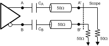 Figure 1. Serializer Test Circuit
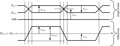 Figure 2. Serializer Output Waveforms
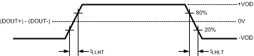 Figure 3. Serializer Output Transition Times
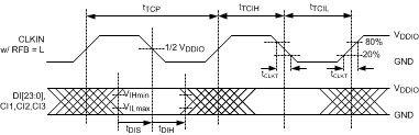 Figure 4. Serializer Input CLKIN Waveform And Set And Hold Times
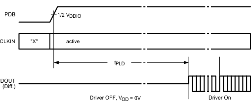 Figure 5. Serializer Lock Time
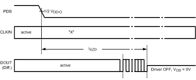 Figure 6. Serializer Disable Time
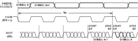 Figure 7. Serializer Latency Delay
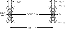 Figure 8. Serializer Output Jitter
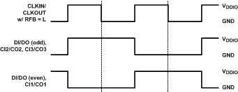 Figure 9. Checkerboard Data Pattern
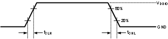 Figure 10. Deserializer LVCMOS Transition Times
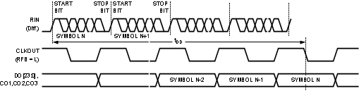 Figure 11. Deserializer Delay – Latency
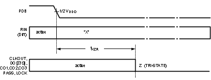 Figure 12. Deserializer Disable Time (OSS_SEL = 0)
 Figure 13. Deserializer PLL Lock Times And PDB Tri-State Delay
 Figure 14. Deserializer Output Data Valid (Setup And Hold) Times With SSCG = Off
 Figure 15. Deserializer Output Data Valid (Setup And Hold) Times With SSCG = On
 Figure 16. Receiver Input Jitter Tolerance
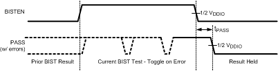 Figure 17. BIST Pass Waveform
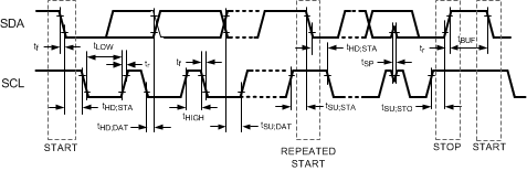 Figure 18. Serial Control Bus Timing Diagram
6.9 Recommended Serializer Timing For CLKIN
Over recommended operating supply and temperature ranges unless otherwise specified.| PARAMETER | TEST CONDITIONS | MIN | TYP | MAX | UNIT | |
|---|---|---|---|---|---|---|
| tTCP | Transmit Input CLKIN Period | 5 MHz to 50 MHz, Figure 4 | 20 | T | 200 | ns |
| tTCIH | Transmit Input CLKIN High Time | 0.4T | 0.5T | 0.6T | ns | |
| tTCIL | Transmit Input CLKIN Low Time | 0.4T | 0.5T | 0.6T | ns | |
| tCLKT | CLKIN Input Transition Time | 0.5 | 2.4 | ns | ||
| SSCIN | CLKIN Input – Spread Spectrum at 50 MHz | fmod | 35 | kHz | ||
| fdev | ±0.02 fMOD |
kHz |
6.10 Serializer Switching Characteristics
Over recommended operating supply and temperature ranges unless otherwise specified.| PARAMETER | TEST CONDITIONS | MIN | TYP | MAX | UNIT | |
|---|---|---|---|---|---|---|
| tLHT | Ser Output Low-to-High Transition Time, Figure 3 | RL = 100Ω, De-emphasis = disabled, VODSEL = 0 |
200 | ps | ||
| RL = 100Ω, De-emphasis = disabled, VODSEL = 1 |
200 | ps | ||||
| tHLT | Ser Output High-to-Low Transition Time, Figure 3 | RL = 100Ω, De-emphasis = disabled, VODSEL = 0 |
200 | ps | ||
| RL = 100Ω, De-emphasis = disabled, VODSEL = 1 |
200 | ps | ||||
| tDIS | Input Data - Setup Time, Figure 4 |
DI[23:0], CI1, CI2, CI3 to CLKIN | 2 | ns | ||
| tDIH | Input Data - Hold Time, Figure 4 |
CLKIN to DI[23:0], CI1, CI2, CI3 | 2 | ns | ||
| tXZD | Ser Output Active to OFF Delay, Figure 6 | 8 | 15 | ns | ||
| tPLD | Serializer PLL Lock Time(5), Figure 5 |
RL = 100Ω | 1.4 | 10 | ms | |
| tSD | Serializer Delay - Latency, Figure 7 | RL = 100Ω | 144*T | 145*T | ns | |
| tDJIT | Ser Output Total Jitter, Figure 8 |
RL = 100Ω, De-Emph = disabled, RANDOM pattern, CLKIN = 50 MHz |
0.28 | UI | ||
| RL = 100Ω, De-Emph = disabled, RANDOM pattern, CLKIN = 43MHz |
0.27 | UI | ||||
| RL = 100Ω, De-Emph = disabled, RANDOM pattern, CLKIN = 5MHz |
0.35 | UI | ||||
| λSTXBW | Serializer Jitter Transfer Function -3 dB Bandwidth |
CLKIN = 50 MHz | 3 | MHz | ||
| CLKIN = 43 MHz | 2.3 | MHz | ||||
| CLKIN = 20 MHz | 1.3 | MHz | ||||
| CLKIN = 5MHz | 650 | kHz | ||||
| δSTX | Serializer Jitter Transfer Function Peaking |
CLKIN = 50 MHz | 0.84 | dB | ||
| CLKIN = 43 MHz | 0.83 | dB | ||||
| CLKIN = 20 MHz | 0.83 | dB | ||||
| CLKIN = 5MHz | 0.28 | dB |
6.11 Deserializer Switching Characteristics
Over recommended operating supply and temperature ranges unless otherwise specified.| PARAMETER | TEST CONDITIONS | PIN/FREQ. | MIN | TYP | MAX | UNIT | |
|---|---|---|---|---|---|---|---|
| tRCP | CLK Output Period | tRCP = tTCP | CLKOUT | 20 | T | 200 | ns |
| tRDC | CLK Output Duty Cycle | SSCG = OFF, 5 – 50MHz | 0.43T | 0.50T | 0.57T | ns | |
| SSCG = ON, 5 – 20 MHz | 0.35T | 0.59T | 0.65T | ns | |||
| SSCG = ON, 20 – 50 MHz | 0.40T | 0.53T | 0.60T | ns | |||
| tCLH | LVCMOS Low-to-High Transition Time, Figure 10 |
VDDIO = 1.8V, CL = 4pF, OS_CLKOUT/DATA = L |
CLKOUT/DO[23:0], CO1, CO2, CO3 | 2.1 | ns | ||
| VDDIO = 3.3V CL = 4pF, OS_CLKOUT/DATA = H |
2.0 | ns | |||||
| tCHL | LVCMOS High-to-Low Transition Time, Figure 10 |
VDDIO = 1.8V CL = 4pF, OS_CLKOUT/DATA = L |
CLKOUT/DO[23:0], CO1, CO2, CO3 | 1.6 | ns | ||
| VDDIO = 3.3V CL = 8 pF, OS_CLKOUT/DATA = H |
1.5 | ns | |||||
| tROS | Data Valid before CLKOUT – Set Up Time, Figure 14 | VDDIO = 1.71 to 1.89V or VDDIO = 3.0 to 3.6V CL = 4pF (lumped load) |
DO[23:0], CO1, CO2, CO3 | 0.27 | 0.45 | T | |
| tROH | Data Valid after CLKOUT – Hold Time, Figure 14 | VDDIO = 1.71 to 1.89V or VDDIO = 3.0 to 3.6V CL = 4pF (lumped load) |
DO[23:0], CO1, CO2, CO3 | 0.4 | 0.55 | T | |
| tDDLT | Deserializer Lock Time, Figure 13 |
SSC[3:0] = OFF, See(6) |
CLKOUT = 5MHz | 3 | ms | ||
| SSC[3:0] = OFF, See(6) |
CLKOUT = 50MHz | 4 | ms | ||||
| SSC[3:0] = ON, See(6) |
CLKOUT = 5MHz | 30 | ms | ||||
| SSC[3:0] = ON, See(6) |
CLKOUT = 50MHz | 6 | ms | ||||
| tDD | Des Delay - Latency, Figure 11 | SSC[3:0] = ON, See(9) |
CLKOUT = 5 to 50 MHz | 139*T | 140*T | ns | |
| tDPJ | Des Period Jitter | SSC[3:0] = OFF, See(8) |
CLKOUT = 5MHz | 975 | 1700 | ps | |
| CLKOUT = 10MHz | 500 | 1000 | ps | ||||
| CLKOUT = 50MHz | 550 | 1250 | ps | ||||
| tDCCJ | Des Cycle-to-Cycle Jitter | SSC[3:0] = OFF, See(9) |
CLKOUT = 5MHz | 675 | 1150 | ps | |
| CLKOUT = 10MHz | 375 | 900 | ps | ||||
| CLKOUT = 50MHz | 500 | 1150 | ps | ||||
| tIIT | Des Input Jitter Tolerance, Figure 16 | EQ = OFF, SSCG = OFF, CLKOUT = 50 MHz |
jitter freq <2MHz | 0.9 | UI(7) | ||
| jitter freq >6MHz | 0.5 | UI(7) | |||||
| BIST MODE | |||||||
| tPASS | BIST PASS Valid Time, BISTEN = 1, Figure 17 |
1 | 10 | µs | |||
| SSCG MODE | |||||||
| fDEV | Spread Spectrum Clocking Deviation Frequency |
Under typical conditions | CLKOUT = 5 to 50 MHz, SSC[3:0] = ON |
±0.005 fMOD | ±0.02 fMOD | KHz | |
| fMOD | Spread Spectrum Clocking Modulation Frequency |
Under typical conditions | CLKOUT = 5 to 50 MHz, SSC[3:0] = ON |
8 | 100 | kHz | |
6.12 Typical Characteristics
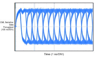
Note: On the rising edge of each clock period, the CML driver outputs a low Stop bit, high Start bit, and 28 DC-scrambled data bits.
Figure 19. Serializer CML Driver Output with 50 MHz TX Pixel Clock.
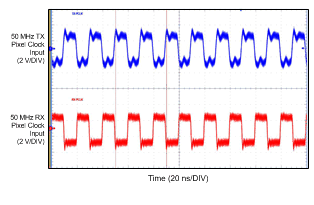
Note: When both devices are locked and the scope is triggered from the TX pixel clock, the RX clock is genlocked to the TX pixel clock and does not drift.
Figure 20. Comparison of Deserializer LVCMOS RX Clock Output locked to a 50 MHz TX Pixel Clock.