JAJSCL7B December   2015  – December 2021 INA300-Q1

PRODUCTION DATA  

  1. 特長
  2. アプリケーション
  3. 概要
  4. Revision History
  5. Pin Configuration and Functions
  6. Specifications
    1. 6.1 Absolute Maximum Ratings
    2. 6.2 ESD Ratings
    3. 6.3 Recommended Operating Conditions
    4. 6.4 Thermal Information
    5. 6.5 Electrical Characteristics
    6. 6.6 Timing Requirements
    7. 6.7 Typical Characteristics
  7. Detailed Description
    1. 7.1 Overview
    2. 7.2 Functional Block Diagram
    3. 7.3 Feature Description
      1. 7.3.1 Selecting a Current-Sensing Resistor
        1. 7.3.1.1 Selecting a Current-Sensing Resistor: Example
      2. 7.3.2 Setting The Current-Limit Threshold
        1. 7.3.2.1 Resistor-Controlled Current Limit
        2. 7.3.2.2 Voltage Source-Controlled Current Limit
      3. 7.3.3 Delay Setting
      4. 7.3.4 Alert Timing Response
      5. 7.3.5 Selectable Hysteresis
      6. 7.3.6 Alert Output
      7. 7.3.7 Noise Adjustment Factor (NAF)
    4. 7.4 Device Functional Modes
      1. 7.4.1 Alert Mode
        1. 7.4.1.1 Transparent Output Mode
        2. 7.4.1.2 Latch Output Mode
      2. 7.4.2 Disable Mode
      3. 7.4.3 Input Filtering
      4. 7.4.4 Using the INA300-Q1 INA300-Q1 With Common-Mode Transients Above 36 V
  8. Application and Implementation
    1. 8.1 Application Information
    2. 8.2 Typical Applications
      1. 8.2.1 Unidirectional Operation
        1. 8.2.1.1 Design Requirements
        2. 8.2.1.2 Detailed Design Procedure
        3. 8.2.1.3 Application Curve
      2. 8.2.2 Bidirectional Operation
        1. 8.2.2.1 Design Requirements
        2. 8.2.2.2 Detailed Design Procedure
        3. 8.2.2.3 Application Curve
      3. 8.2.3 Window Comparator
        1. 8.2.3.1 Design Requirements
        2. 8.2.3.2 Detailed Design Procedure
        3. 8.2.3.3 Application Curve
  9. Power Supply Recommendations
  10. 10Layout
    1. 10.1 Layout Guidelines
    2. 10.2 Layout Example
  11. 11Device and Documentation Support
    1. 11.1 Documentation Support
      1. 11.1.1 Related Documentation
    2. 11.2 Receiving Notification of Documentation Updates
    3. 11.3 サポート・リソース
    4. 11.4 Trademarks
    5. 11.5 Electrostatic Discharge Caution
    6. 11.6 Glossary
  12. 12Mechanical, Packaging, and Orderable Information

パッケージ・オプション

メカニカル・データ(パッケージ|ピン)
サーマルパッド・メカニカル・データ
発注情報

Pin Configuration and Functions

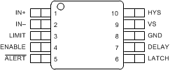
GUID-1525EDC8-DA4A-48A7-BDAF-8892860CB2FC-low.gifFigure 5-1 DGS Package10-Pin VSSOPTop View
Table 5-1 Pin Functions
PIN I/O DESCRIPTION
NO. NAME
1 IN+ Analog input Connect to supply side of shunt resistor.
2 IN– Analog input Connect to load side of shunt resistor.
3 LIMIT Analog input Alert threshold limit input.
See Section 7.3.2 for details on setting limit threshold.
4 ENABLE Digital input Enable or disable selection input
5 ALERT Digital output Overlimit alert, active-low, open-drain output.
6 LATCH Digital input Transparent or latch mode selection input.
7 DELAY Digital input Response time selection input.
8 GND Analog Ground
9 VS Analog Power supply, 2.7 V to 5.5 V.
10 HYS Digital input Hysteresis setting input.
See Section 7.3.5 for hysteresis settings.