JAJSHG3 May   2018 LM3102-Q1

PRODUCTION DATA.  

  1. 特長
  2. アプリケーション
  3. 概要
    1.     Device Images
      1.      代表的なアプリケーションの回路図
      2.      効率と負荷電流との関係(VOUT=3.3V)
  4. 改訂履歴
  5. Pin Configuration and Functions
    1.     Pin Functions
  6. Specifications
    1. 6.1 Absolute Maximum Ratings
    2. 6.2 ESD Ratings
    3. 6.3 Recommended Operating Conditions
    4. 6.4 Thermal Information
    5. 6.5 Electrical Characteristics
    6. 6.6 Switching Characteristics
    7. 6.7 Typical Characteristics
  7. Detailed Description
    1. 7.1 Overview
    2. 7.2 Functional Block Diagram
    3. 7.3 Feature Description
      1. 7.3.1  COT Control Circuit Overview
      2. 7.3.2  Start-Up Regulator (VCC)
      3. 7.3.3  Regulation Comparator
      4. 7.3.4  Zero Coil Current Detect
      5. 7.3.5  Overvoltage Comparator
      6. 7.3.6  Current Limit
      7. 7.3.7  N-Channel MOSFET and Driver
      8. 7.3.8  Soft Start
      9. 7.3.9  Thermal Protection
      10. 7.3.10 Thermal Derating
    4. 7.4 Device Functional Modes
      1. 7.4.1 ON-Time Timer, Shutdown
  8. Application and Implementation
    1. 8.1 Application Information
    2. 8.2 Typical Application
      1. 8.2.1 Design Requirements
      2. 8.2.2 Detailed Design Procedure
        1. 8.2.2.1 Custom Design With WEBENCH® Tools
        2. 8.2.2.2 Design Steps for the LM3102-Q1 Application
        3. 8.2.2.3 External Components
      3. 8.2.3 Application Curve
    3. 8.3 System Examples
  9. Power Supply Recommendations
  10. 10Layout
    1. 10.1 Layout Guidelines
    2. 10.2 Layout Example
  11. 11デバイスおよびドキュメントのサポート
    1. 11.1 デバイス・サポート
      1. 11.1.1 開発サポート
        1. 11.1.1.1 WEBENCH®ツールによるカスタム設計
    2. 11.2 ドキュメントの更新通知を受け取る方法
    3. 11.3 コミュニティ・リソース
    4. 11.4 商標
    5. 11.5 静電気放電に関する注意事項
    6. 11.6 Glossary
  12. 12メカニカル、パッケージ、および注文情報

パッケージ・オプション

メカニカル・データ(パッケージ|ピン)
サーマルパッド・メカニカル・データ
発注情報

Pin Configuration and Functions

PWP Package
20-Pin HTSSOP
Top View
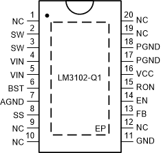
LM3102-Q1 30021302.gif

Pin Functions

PIN TYPE DESCRIPTION
NAME NO.
N/C 1 No Connection
9
10
12
19
20
SW 2 Power Switching node
3
VIN 4 Power Input supply voltage
5
BST 6 Power Connection for bootstrap capacitor
AGND 7 Ground Analog ground
SS 8 Analog Soft start
GND 11 Ground Ground
FB 13 Analog Feedback
EN 14 Analog Enable
RON 15 Analog ON-time control
VCC 16 Power Start-up regulator output
PGND 17 Ground Power ground
18
EP Ground Exposed Pad