JAJSBJ7H June 2009 – September 2016 LM5009A
PRODUCTION DATA.
- 1 特長
- 2 アプリケーション
- 3 概要
- 4 改訂履歴
- 5 Pin Configuration and Functions
- 6 Specifications
- 7 Detailed Description
- 8 Application and Implementation
- 9 Power Supply Recommendations
- 10Layout
- 11デバイスおよびドキュメントのサポート
- 12メカニカル、パッケージ、および注文情報
パッケージ・オプション
メカニカル・データ(パッケージ|ピン)
サーマルパッド・メカニカル・データ
発注情報
10 Layout
10.1 Layout Guidelines
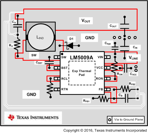
The LM5009A regulation and overvoltage comparators are very fast, and as such respond to short duration noise pulses. Therefore, layout considerations are critical for optimum performance. The components at pins 1, 2, 3, 5, and 6 must be as physically close as possible to the IC, thereby minimizing noise pickup in the PC tracks. The current loop formed by D1, L1, and C2 must be as small as possible. The ground connection from D1 to C1 must be as short and direct as possible.
If the internal dissipation of the LM5009A produces excessive junction temperatures during normal operation, good use of the PCB ground plane can help to dissipate heat. The exposed pad on the bottom of the 8-pin WSON package is soldered to a ground plane on the PCB, and that plane must extend out from beneath the IC to help dissipate the heat. Additionally, the use of wide PCB traces, where possible, can also help conduct heat away from the IC. Judicious positioning of the PCB within the end product, along with use of any available air flow (forced or natural convection) can help reduce the junction temperatures.
10.2 Layout Example
 Figure 13. LM5009A Buck Layout Example With the WSON Package