JAJSBJ7H June 2009 – September 2016 LM5009A
PRODUCTION DATA.
- 1 特長
- 2 アプリケーション
- 3 概要
- 4 改訂履歴
- 5 Pin Configuration and Functions
- 6 Specifications
- 7 Detailed Description
- 8 Application and Implementation
- 9 Power Supply Recommendations
- 10Layout
- 11デバイスおよびドキュメントのサポート
- 12メカニカル、パッケージ、および注文情報
パッケージ・オプション
メカニカル・データ(パッケージ|ピン)
サーマルパッド・メカニカル・データ
発注情報
7 Detailed Description
7.1 Overview
The LM5009A device is a step-down switching regulator featuring all of the functions required to implement a low-cost, efficient, buck bias power converter. This high-voltage regulator contains a 100-V, N-channel buck switch, is easy to implement, and is provided in the 8-pin VSSOP and the thermally-enhanced, 8-pin WSON packages. The regulator is based on a control scheme using an ON time inversely proportional to VIN. The control scheme requires no loop compensation. Current limit is implemented with forced OFF time, which is inversely proportional to VOUT. This scheme ensures short circuit control while providing minimum foldback.
The LM5009A is applied in numerous applications to efficiently regulate down higher voltages. This regulator is well suited for 48-V Telecom and the new 42-V Automotive power bus ranges.
7.2 Functional Block Diagram

7.3 Feature Description
7.3.1 Control Circuit Overview
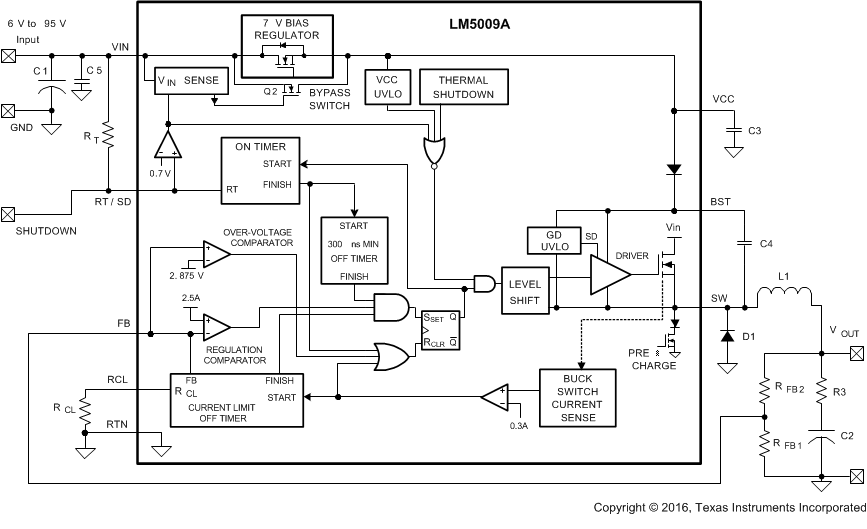
The LM5009A is a buck DC-DC regulator that uses a control scheme in which the ON time varies inversely with line voltage (VIN). Control is based on a comparator and the ON-time one-shot, with the output voltage feedback (FB) compared to an internal reference (2.5 V). If the FB level is below the reference the buck switch is turned on for a fixed time determined by the line voltage and a programming resistor (RT). Following the ON period the switch remains off for at least the minimum off-timer period of 300 ns. If FB is still below the reference at that time, the switch turns on again for another ON-time period. This continues until regulation is achieved.
The LM5009A operates in discontinuous conduction mode at light load currents, and continuous conduction mode at heavy load current. In discontinuous conduction mode, current through the output inductor starts at zero and ramps up to a peak during the ON time, then ramps back to zero before the end of the OFF time. The next ON-time period starts when the voltage at FB falls below the internal reference; until then, the inductor current remains zero. In this mode, the operating frequency is lower than in continuous conduction mode, and varies with load current. Therefore, at light loads the conversion efficiency is maintained, because the switching losses reduce with the reduction in load and frequency. The discontinuous operating frequency is calculated with Equation 1.

where
- RL = the load resistance
In continuous conduction mode, current flows continuously through the inductor and never ramps down to zero. In this mode the operating frequency is greater than the discontinuous mode frequency and remains relatively constant with load and line variations. The approximate continuous mode operating frequency is calculated with Equation 2.

The output voltage (VOUT) is programmed by two external resistors as shown in Functional Block Diagram. The regulation point is calculated with Equation 3.
The LM5009A regulates the output voltage based on ripple voltage at the feedback input, requiring a minimum amount of ESR for the output capacitor C2. A minimum of 25 mV to 50 mV of ripple voltage at the feedback pin (FB) is required for the LM5009A. In cases where the capacitor ESR is too small, additional series resistance may be required (R3 in Functional Block Diagram).
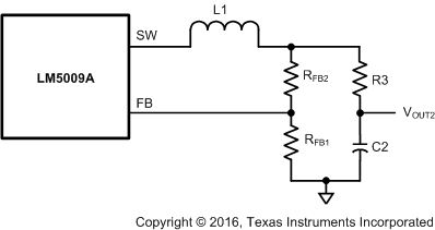
For applications where lower output voltage ripple is required, the output is taken directly from a low-ESR output capacitor, as shown in Figure 7. However, R3 slightly degrades the load regulation.
 Figure 7. Low Ripple Output Configuration
7.3.2 Start-Up Regulator (VCC)
The high-voltage bias regulator is integrated within the LM5009A. The input pin (VIN) is connected directly to line voltages between 6 V and 95 V, with transient capability to 100 V. Referring to Functional Block Diagram and Figure 2, when VIN is between 6 V and the bypass threshold (nominally 8.5 V), the bypass switch (Q2) is on, and VCC tracks VIN within 100 mV to 150 mV. The bypass switch on-resistance is approximately 100 Ω, with inherent current limiting at approximately 100 mA. When VIN is above the bypass threshold Q2 is turned off, and VCC is regulated at 7 V. The VCC regulator output current is limited at approximately 9.2 mA. When the LM5009A is shutdown using the RT/SD pin, the VCC bypass switch is shut off regardless of the voltage at VIN.
When VIN exceeds the bypass threshold, the time required for Q2 to shut off is approximately 2 µs to 3 µs. The capacitor at VCC (C3) must be a minimum of 0.47 µF to prevent the voltage at VCC from rising above the absolute maximum rating in response to a step input applied at VIN. C3 must be placed as close as possible to the VCC and RTN pins. In applications with a relatively high input voltage, power dissipation in the bias regulator is a concern. An auxiliary voltage of between 7.5 V and 14 V is diode connected to the VCC pin to shut off the VCC regulator, thereby reducing internal power dissipation. The current required into the VCC pin is shown in Figure 6. Internally a diode connects VCC to VIN requiring that the auxiliary voltage be less than VIN.
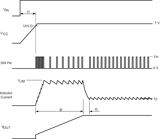
The turnon sequence is shown in Figure 8. During the initial delay (t1) VCC ramps up at a rate determined by the current limit and C3 while internal circuitry stabilizes. When VCC reaches UVLO (typically 5.3 V) the buck switch is enabled. The inductor current increases to the current limit threshold (ILIM) and during t2 VOUT increases as the output capacitor charges up. When VOUT reaches the intended voltage, the average inductor current decreases (t3) to the nominal load current (IO).
 Figure 8. Start-Up Sequence
7.3.3 Regulation Comparator
The feedback voltage at FB is compared to an internal 2.5-V reference. In normal operation (the output voltage is regulated), an ON-time period is initiated when the voltage at FB falls below 2.5 V. The buck switch stays on for the ON time, causing the FB voltage to rise above 2.5 V. After the ON-time period, the buck switch stays off until the FB voltage again falls below 2.5 V. During start-up, the FB voltage is below 2.5 V at the end of each ON time, resulting in the minimum OFF-time of 300 ns. Bias current at the FB pin is nominally 100 nA.
7.3.4 Overvoltage Comparator
The feedback voltage at FB is compared to an internal 2.875-V reference. If the voltage at FB rises above
2.875 V, the ON-time pulse is immediately terminated. This condition can occur if the input voltage or the output load change suddenly. The buck switch does not turn on again until the voltage at FB falls below 2.5 V.
7.3.5 ON-Time Generator and Shutdown
The ON time for the LM5009A is determined by the RT resistor, and is inversely proportional to the input voltage (VIN). This results in a nearly constant frequency as VIN is varied over the VIN range. The ON-time equation for the LM5009A is calculated with Equation 4.
RT must be selected for a minimum ON time (at maximum VIN) greater than 400 ns, for proper current limit operation. This requirement limits the maximum frequency for each application, depending on VIN and VOUT.
7.3.6 Current Limit
The LM5009A contains an intelligent current limit OFF timer. If the current in the Buck switch exceeds 0.3 A, the present cycle is immediately terminated, and a non-resetable OFF timer is initiated. The length of OFF time is controlled by an external resistor (RCL) and the FB voltage (see Figure 4). When FB = 0 V, a maximum OFF time is required, and the time is preset to 35 µs. This condition occurs when the output is shorted, and during the initial part of start-up. This amount of time ensures safe short circuit operation up to the maximum input voltage of
95 V. In cases of overload where the FB voltage is above 0 V (not a short circuit), the current limit OFF time is less than 35 µs. Reducing the OFF time during less severe overloads reduces the amount of foldback, recovery time, and the start-up time. The OFF time is calculated with Equation 5.

The current limit sensing circuit is blanked for the first 50 ns to 70 ns of each ON time, so it is not falsely tripped by the current surge which occurs at turnon. The current surge is required by the recirculating diode (D1) for the turnoff recovery.
7.3.7 N-Channel Buck Switch and Driver
The LM5009A integrates an N-channel Buck switch and associated floating high-voltage gate driver. The gate driver circuit works in conjunction with an external bootstrap capacitor and an internal high voltage diode. A
0.01-µF ceramic capacitor (C4) connected between the BST pin and SW pin provides the voltage to the driver during the ON time.
During each OFF time, the SW pin is at approximately 0 V, and the bootstrap capacitor charges from VCC through the internal diode. The minimum OFF timer, set to 300 ns, ensures a minimum time each cycle to recharge the bootstrap capacitor.
The internal precharge switch at the SW pin is turned on for approximately 150 ns during the minimum OFF-time period, ensuring sufficient voltage exists across the bootstrap capacitor for the ON time. This feature helps prevent operating problems which can occur during very light-load conditions, involving a long OFF time, during which the voltage across the bootstrap capacitor could otherwise reduce below the gate drive UVLO threshold. The precharge switch also helps prevent start-up problems which can occur if the output voltage is precharged prior to turnon. After current limit detection, the precharge switch is turned on for the entire duration of the forced OFF time.
7.3.8 Thermal Protection
The LM5009A must be operated so the junction temperature does not exceed 125°C during normal operation. An internal thermal shutdown circuit is provided to shutdown the LM5009A in the event of a higher than normal junction temperature. When activated, typically at 165°C, the controller is forced into a low power reset state by disabling the buck switch. This feature prevents catastrophic failures from accidental device overheating. When the junction temperature reduces below 140°C, normal operation is resumed (typical hysteresis = 25°C).
7.4 Device Functional Modes
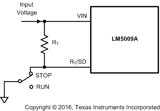
The LM5009A is remotely disabled by taking the RT/SD pin to ground, as shown in Figure 9. The voltage at the RT/SD pin is between 1.5 V and 3 V, depending on VIN and the value of the RT resistor.
 Figure 9. Shutdown Implementation