SNVS428H January 2006 – October 2015 LM5035
PRODUCTION DATA.
- 1 Features
- 2 Applications
- 3 Description
- 4 Revision History
- 5 Pin Configuration and Functions
- 6 Specifications
-
7 Detailed Description
- 7.1 Overview
- 7.2 Functional Block Diagram
- 7.3
Feature Description
- 7.3.1 High-Voltage Start-Up Regulator
- 7.3.2 Line Undervoltage Detector
- 7.3.3 Line Overvoltage, Load Overvoltage, Remote Thermal Protection
- 7.3.4 Reference
- 7.3.5 Cycle-by-Cycle Current Limit
- 7.3.6 Overload Protection Timer
- 7.3.7 Soft-Start
- 7.3.8 Soft-Stop
- 7.3.9 PWM Comparator
- 7.3.10 Feedforward Ramp and Volt-Second Clamp
- 7.3.11 Oscillator, Sync Capability
- 7.3.12 Gate-Driver Outputs (HO and LO)
- 7.3.13 Synchronous Rectifier Control Outputs (SR1 and SR2)
- 7.3.14 Thermal Protection
- 7.4 Device Functional Modes
- 8 Application and Implementation
- 9 Power Supply Recommendations
- 10Layout
- 11Device and Documentation Support
- 12Mechanical, Packaging, and Orderable Information
パッケージ・オプション
メカニカル・データ(パッケージ|ピン)
サーマルパッド・メカニカル・データ
- PWP|20
発注情報
8 Application and Implementation
NOTE
Information in the following applications sections is not part of the TI component specification, and TI does not warrant its accuracy or completeness. TI’s customers are responsible for determining suitability of components for their purposes. Customers must validate and test their design implementation to confirm system functionality.
8.1 Application Information
The following information is intended to provide guidelines for the power-supply designer using the LM5035.
8.2 Typical Application
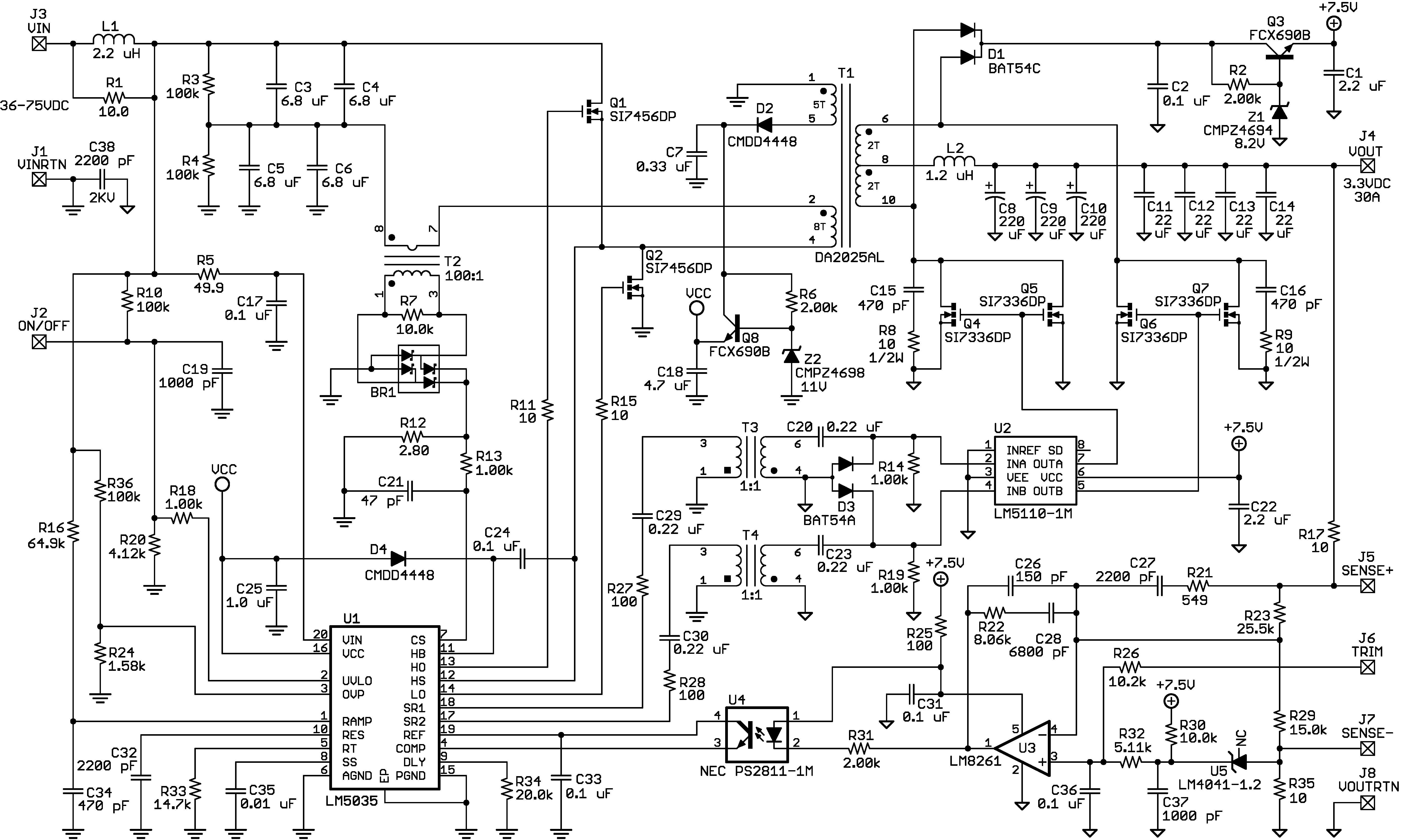
Figure 15 shows an example of a 100-W half-bridge power converter controlled by the LM5035. The operating input-voltage range (VPWR) is 36 V to 75 V, and the output voltage is 3.3 V. The output-current capability is 30 A. Current sense transformer T2 provides information to the CS pin for current-limit protection. The error amplifier and reference, U3 and U5 respectively, provide voltage feedback through optocoupler U4. Synchronous rectifiers (Q4, Q5, Q6, and Q7) minimize rectification losses in the secondary. An auxiliary winding on transformer T1 provides power to the LM5035 VCC pin when the output is in regulation. The input voltage UVLO thresholds are ≊ 34 V for increasing VPWR, and ≊ 32 V for decreasing VPWR. The circuit can be shut down by driving the ON/OFF input (J2) below 1.25 V with an open-collector or open-drain circuit. An external synchronizing frequency can be applied through a 100-pF capacitor to the RT input (U1 pin 5). The regulator output is current limited at ≊ 34 A.
8.2.1 Design Requirements
Table 1 lists example design parameters for the application circuit layout in Figure 15.
Table 1. Design Parameters
| PARAMETER | MIN | NOM | MAX | UNIT |
|---|---|---|---|---|
| Input voltage (VIN) | 36 | 72 | V | |
| Output voltage (VOUT) | 3.3 | V | ||
| Output current (IOUT) | 0 | 30 | A | |
| Switching frequency | 400 | kHz | ||
| Efficiency (full load) | 89% | |||
| Efficiency (half load) | 92% | |||
| Load regulation | 0.2% | |||
| Line regulation | 0.1% | |||
| undervoltage lock-out (ON) | 33.9 | V | ||
| undervoltage lock-out (OFF) | 31.9 | V | ||
| Line overvoltage protection (ON) | 79.4 | V | ||
| Line overvoltage protection (OFF) | 78.3 | V |
8.2.2 Detailed Design Procedure
8.2.2.1 VIN
The voltage applied to the VIN pin, which may be the same as the system voltage applied to the power transformer primary (VPWR), can vary in the range from 13 V to 105 V. The current into VIN depends primarily on the gate charge provided to the output drivers, the switching frequency, and any external loads on the VCC and REF pins. It is recommended the filter shown in Figure 16 be used to suppress transients which may occur at the input supply. This is particularly important when VIN is operated close to the maximum operating rating of the LM5035.
When power is applied to VIN and the UVLO pin voltage is greater than 0.4 V, the VCC regulator is enabled and supplies current into an external capacitor connected to the VCC pin. When the voltage on the VCC pin reaches the regulation point of 7.6 V, the voltage reference (REF) is enabled. The reference regulation set point is 5 V. The HO, LO, SR1, and SR2 outputs are enabled when the two bias regulators reach their set point and the UVLO pin potential is greater than 1.25 V. In typical applications, an auxiliary transformer winding is connected through a diode to the VCC pin. This winding must raise the VCC voltage above 8.3 V to shut off the internal start-up regulator.
After the outputs are enabled and the external VCC supply voltage has begun supplying power to the IC, the current into VIN drops below 1 mA. VIN must remain at a voltage equal to or above the VCC voltage to avoid reverse current through protection diodes.
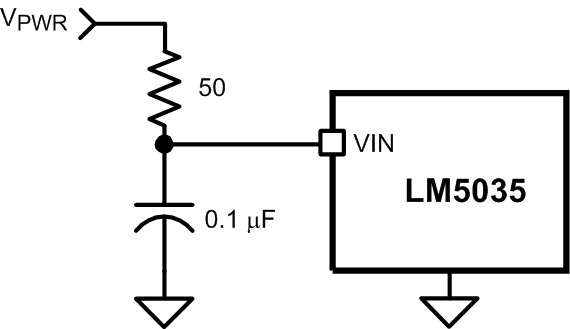 Figure 16. Input-Transient Protection
8.2.2.2 For Applications >100 V
For applications where the system input voltage exceeds 100 V or the IC power dissipation is of concern, the LM5035 can be powered from an external start-up regulator as shown in Figure 17. In this configuration, the VIN and the VCC pins must be connected together, which allows the LM5035 to be operated below 13 V. The voltage at the VCC pin must be greater than 8.3 V, yet not exceed 15 V. An auxiliary winding can be used to reduce the power dissipation in the external regulator once the power converter is active. The NPN base-emitter reverse breakdown voltage, which can be as low as 5 V for some transistors, must be considered when selecting the transistor.
8.2.2.3 Current Sense
The CS pin needs to receive an input signal representative of the primary current of the transformer, either from a current sense transformer or from a resistor in series with the source of the LO switch, as shown in Figure 18 and Figure 19. In both cases, the sensed current creates a ramping voltage across R1, and the RF / CF filter suppresses noise and transients. R1, RF and CF must be located as close to the LM5035 as possible, and the ground connection from the current sense transformer, or R1, must be a dedicated track to the AGND pin. The current sense components must provide greater than 0.25 V at the CS pin when an overcurrent condition exists.
 Figure 17. Start-Up Regulator for VPWR >100 V
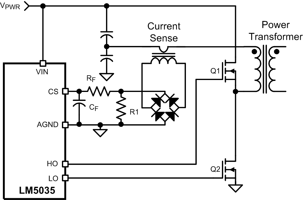 Figure 18. Current Sense Using Current Sense Transformer
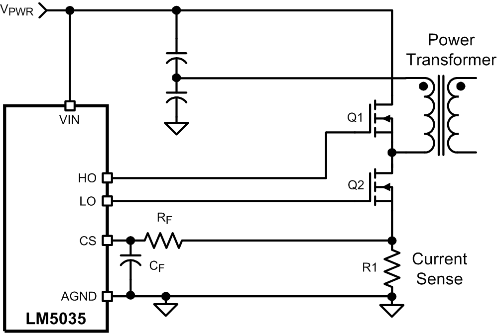 Figure 19. Current Sense Using Current Sense Resistor (R1)
If the current sense resistor method is used, the overcurrent condition will only be sensed while LO is driving the low-side MOSFET. Overcurrent while HO is driving the high-side MOSFET will not be detected. In this configuration, it will take 4 times as long for continuous cycle-by-cycle current limiting to initiate a restart event since each overcurrent event during LO enables the 22-µA RES pin current source for one oscillator period, and then the lack of an overcurrent event during HO enables the 12-µA RES pin current sink for one oscillator period. The time average of this toggling is equivalent to a continuous 5-µA current source into the RES capacitor, increasing the delay by a factor of four. The value of the RES capacitor can be reduced to decrease the time before restart cycle is initiated.
When using the resistor current sense method, an imbalance in the input capacitor voltages may develop when operating in cycle-by-cycle current limiting mode. If the imbalance persists for an extended period, excessive currents in the non-sensed MOSFET, and possible transformer saturation may result. This condition is inherent to the half-bridge topology operated with cycle-by-cycle current limiting and is compounded by only sensing in one leg of the half-bridge circuit. The imbalance is greatest at large duty cycles (low input voltages). If using this method, it is recommended that the capacitor on the RES pin be no larger than 220 pF. Check the final circuit and reduce the RES capacitor further, or omit the capacitor completely to ensure the voltages across the bridge capacitors remain balanced. The current limit value may decrease slightly as the RES capacitor is reduced.
8.2.2.4 HO, HB, HS, and LO
Attention must be given to the PC board layout for the low-side driver and the floating high-side driver pins HO, HB and HS. A low ESR or ESL capacitor (such as a ceramic surface mount capacitor) must be connected close to the LM5035, between HB and HS to provide high peak currents during turnon of the high-side MOSFET. The capacitor must be large enough to supply the MOSFET gate charge (Qg) without discharging to the point where the drop in gate voltage affects the MOSFET RDS(ON). Use Equation 6 to calculate the value for CBOOST. A value that is ten to 20 times Qg is recommended.

The diode (DBOOST) that charges CBOOST from VCC when the low-side MOSFET is conducting must be capable of withstanding the full converter input voltage range. When the high-side MOSFET is conducting, the reverse voltage at the diode is approximately the same as the MOSFET drain voltage because the high-side driver is boosted up to the converter input voltage by the HS pin, and the high side MOSFET gate is driven to the HS voltage plus VCC. Since the anode of DBOOST is connected to VCC, the reverse potential across the diode is equal to the input voltage minus the VCC voltage. DBOOST average current is less than 20 mA in most applications, so a low current ultra-fast recovery diode is recommended to limit the loss due to diode junction capacitance. Schottky diodes are also a viable option, particularly for lower input voltage applications, but attention must be paid to leakage currents at high temperatures.
The internal gate drivers need a very low impedance path to the respective decoupling capacitors; the VCC cap for the LO driver and CBOOST for the HO driver. These connections must be as short as possible to reduce inductance and as wide as possible to reduce resistance. The loop area, defined by the gate connection and its respective return path, must be minimized.
The high-side gate driver can also be used with HS connected to PGND for applications other than a half bridge converter (for example, push-pull). The HB pin is then connected to VCC, or any supply greater than the high-side driver undervoltage lockout (approximately 6.5 V). In addition, the high-side driver can be configured for high voltage offline applications where the high-side MOSFET gate is driven via a gate drive transformer.
8.2.2.5 Programmable Delay (DLY)
The RDLY resistor programs the delays between the SR1 and SR2 signals and the HO and LO driver outputs. Figure 14 shows the relationship between these outputs. The DLY pin is nominally set at 2.5 V and the current is sensed through RDLY to ground. This current is used to adjust the amount of dead time before the HO and LO pulse (T1) and after the HO and LO pulse (T2). Typically RDLY is in the range of 10 kΩ to 100 kΩ. The dead-time periods can be calculated using Equation 7 and Equation 8:
T1 and T2 can be set to minimum by not connecting a resistor to DLY, connecting a resistor greater than 300 kΩ from DLY to ground, or connecting DLY to the REF pin. This may cause lower than optimal system efficiency if the delays through the SR signal transformer network, the secondary gate drivers and the SR MOSFETs are greater than the delay to turn on the HO or LO MOSFETs. must an SR MOSFET remain on while the opposing primary MOSFET is supplying power through the power transformer, the secondary winding will experience a momentary short circuit, causing a significant power loss to occur.
When choosing the RDLY value, worst case propagation delays and component tolerances must be considered to assure that there is never a time where both SR MOSFETs are enabled AND one of the primary side MOSFETs is enabled. The time period T1 must be set so that the SR MOSFET has turned off before the primary MOSFET is enabled. Conversely, T1 and T2 must be kept as low as tolerances allow to optimize efficiency. The SR body diode conducts during the time between the SR MOSFET turns off and the power transformer begins supplying energy. Power losses increase when this happens since the body diode voltage drop is many times higher than the MOSFET channel voltage drop. The interval of body diode conduction can be observed with an oscilloscope as a negative 0.7 V to 1.5 V pulse at the SR MOSFET drain.
8.2.2.6 UVLO and OVP Voltage Divider Selection for R1, R2, and R3
Two dedicated comparators connected to the UVLO and OVP pins are used to detect undervoltage and overvoltage conditions. The threshold value of these comparators, VUVLO and VOVP, is 1.25 V (typical). The two functions can be programmed independently with two voltage dividers from VIN to AGND as shown in Figure 20 and Figure 21, or with a three-resistor divider as shown in Figure 22. Independent UVLO and OVP pins provide greater flexibility for the user to select the operational voltage range of the system. Hysteresis is accomplished by 23-µA current sources (IUVLO and IOVP), which are switched on or off into the sense pin resistor dividers as the comparators change state.
When the UVLO pin voltage is below 0.4 V, the controller is in a low current shutdown mode. For a UVLO pin voltage greater than 0.4 V but less than 1.25 V the controller is in standby mode. Once the UVLO pin voltage is greater than 1.25 V, the controller is fully enabled. Two external resistors can be used to program the minimum operational voltage for the power converter as shown in Figure 20. When the UVLO pin voltage falls below the 1.25-V threshold, an internal 23-µA current sink is enabled to lower the voltage at the UVLO pin, thus providing threshold hysteresis. Resistance values for R1 and R2 can be determined from Equation 9 and Equation 10.


where
- VPWR is the desired turnon voltage
- VHYS is the desired UVLO hysteresis at VPWR
For example, if the LM5035 is to be enabled when VPWR reaches 34 V, and disabled when VPWR is decreased to 32 V, R1 must be 87 kΩ, and R2 must be 3.54 kΩ. The voltage at the UVLO pin must not exceed 7 V at any time. Be sure to check both the power and voltage rating (0603 resistors can be rated as low as 50 V) for the selected R1 resistor.
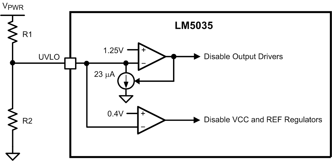 Figure 20. Basic UVLO Configuration
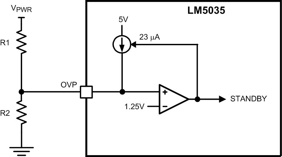 Figure 21. Basic Overvoltage Protection
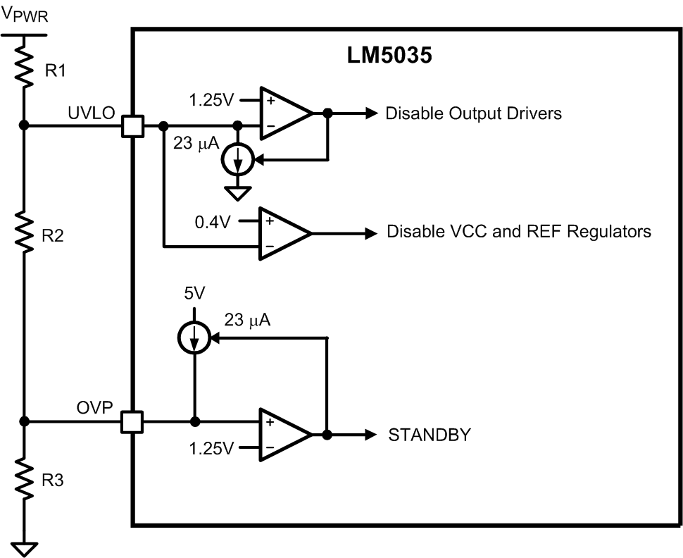 Figure 22. UVLO and OVP Divider
The impedance seen looking into the resistor divider from the UVLO and OVP pins determines the hysteresis level. UVLO and OVP enable and disable thresholds are calculated using the equations in Table 2 for the three-resistor divider listed in Figure 22.
Table 2. UVO and OVP Divider Formulas
| THRESHOLD | EQUATION |
|---|---|
| Outputs disabled due to VIN falling below UVLO threshold |
Equation 11.
 |
| Outputs enabled due to VIN rising above UVLO threshold | UVLOon = UVLOoff + (23 µA × R1) |
| Outputs disabled due to VIN rising above OVP threshold |
Equation 12.
 |
| Outputs enabled due to VIN falling below OVP threshold | OVPon = OVPoff – [23 µA × (R1 + R2)] |
The equations listed in Table 2 calculate the typical operating ranges of undervoltage and overvoltage thresholds. For example, for resistor values R1 = 86.6 kΩ, R2 = 2.1 kΩ and R3 = 1.4 kΩ the calculated thresholds are as follows:
- UVLO turnoff = 32.2 V
- UVLO turnon = 34.2 V
- OVP turnon = 78.4 V
- OVP turnoff = 80.5 V
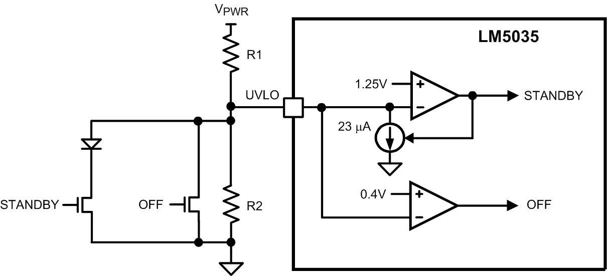 Figure 23. Remote Standby and Disable Control
To maintain the accuracy of the threshold, a resistor tolerance of 1% or better is recommended.
The design process begins with the selection of the voltage difference between the UVLO enabling and disabling thresholds. This selection also sets the approximate difference between OVP enabling and disabling regulation. Use Equation 13 to calculate the value of R1.

Next, the combined resistance of R2 and R3 is calculated by selecting the threshold for the UVLO disabling threshold. Use Equation 14 to calculate the value of RCOMBINED.

The value of R3 is then determined by selecting the OVP disabling threshold. Use Equation 15 to calculate the value of R3.

Finally, subtract the value of R3 from the value of RCOMBINED calculate the value of R2 as shown in Equation 16.
Remote configuration of the operational modes of the controller can be accomplished with open drain devices connected to the UVLO pin as shown in Figure 23.
8.2.2.7 Fault Protection
The overvoltage protection (OVP) comparator of the LM5035 can be configured for line or load fault protection or thermal protection using an external temperature sensor or thermistor. Figure 21 shows a line over voltage shutdown application using a voltage divider between the input power supply, VPWR, and AGND to monitor the line voltage.
Figure 24 demonstrates the use of the OVP pin for latched output overvoltage fault protection, using a zener and optocoupler. When VOUT exceeds the conduction threshold of the optocoupler diode and zener, the optocoupler momentarily turns on Q1 and the LM5035 enters standby mode, disabling the drivers and enabling the hysteresis current source on the OVP pin. When the current source is enabled, the OVP voltage will remain at 2.3 V (23 µA × 100 kΩ) without additional drive from the external circuit. If the optocoupler transistor emitter were directly connected to the OVP pin, then leakage current in the zener diode amplified by the gain of the optocoupler could falsely trip the protection latch. R1 and Q1 are added reduce the sensitivity to low level currents in the optocoupler. Using the values of Figure 24, the optocoupler collector current must equal VBE(Q1) / R1 = 350 µA before OVP latches. Once the controller has switched to standby mode, the outputs no longer switch but the VCC and REF regulators continue functioning and supply bias to the external circuitry. VCC must fall below 6.2 V or the UVLO pin must fall below 0.4 V to clear the OVP latch.
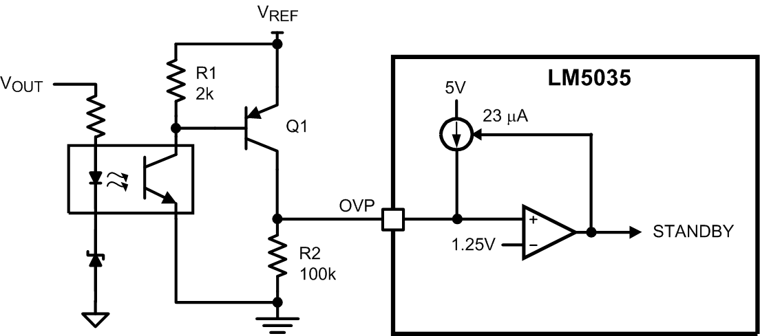 Figure 24. Latched Load Overvoltage Protection
Figure 25 shows an application of the OVP comparator for Remote Thermal Protection using a thermistor (or multiple thermistors) which may be located near the main heat sources of the power supply. The negative temperature coefficient (NTC) thermistor is nearly logarithmic, and in this example a 100kΩ thermistor with the β material constant of 4500 kelvins changes to approximately 2 kΩ at 130°C. Setting R1 to one-third of this resistance (665 Ω) establishes 130°C as the desired trip point (for VREF = 5 V). In a temperature band from 20°C below to 20°C above the OVP threshold, the voltage divider is nearly linear with 25 mV per°C sensitivity.
R2 provides temperature hysteresis by raising the OVP comparator input by R2 × 23 µA. For example, if a 22-kΩ resistor is selected for R2, then the OVP pin voltage will increase by 22 kΩ × 23 µA = 506 mV. The NTC temperature must therefore fall by 506 mV / 25 mV per°C = 20°C before the LM5035 switches from the standby mode to the normal mode.
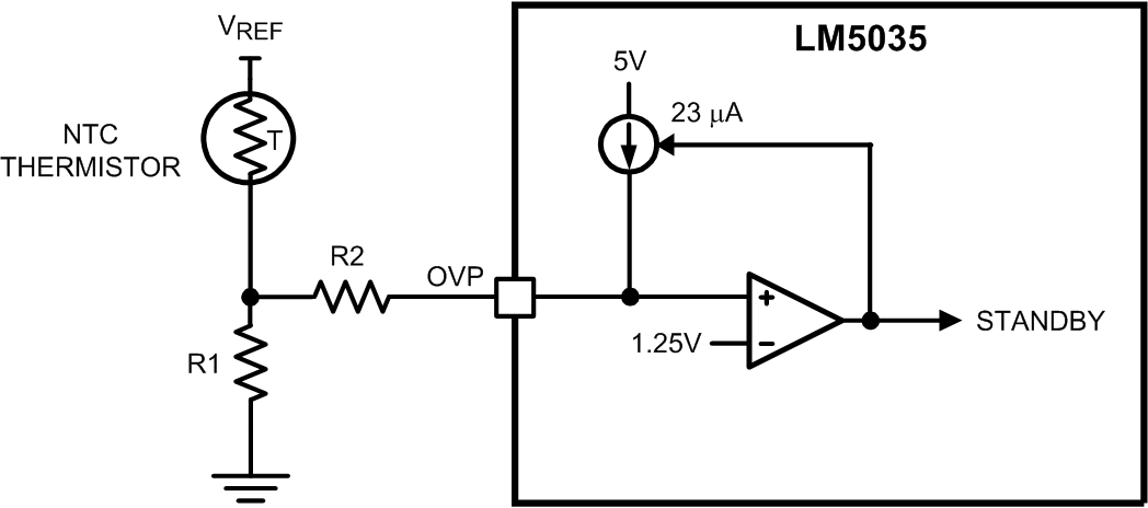 Figure 25. Remote Thermal Protection
8.2.2.8 HICCUP Mode Current-Limit Restart (RES)
The basic operation of the hiccup mode current limit restart is described in the functional description. The delay time to restart is programmed with the selection of the RES pin capacitor CRES as shown in Figure 25.
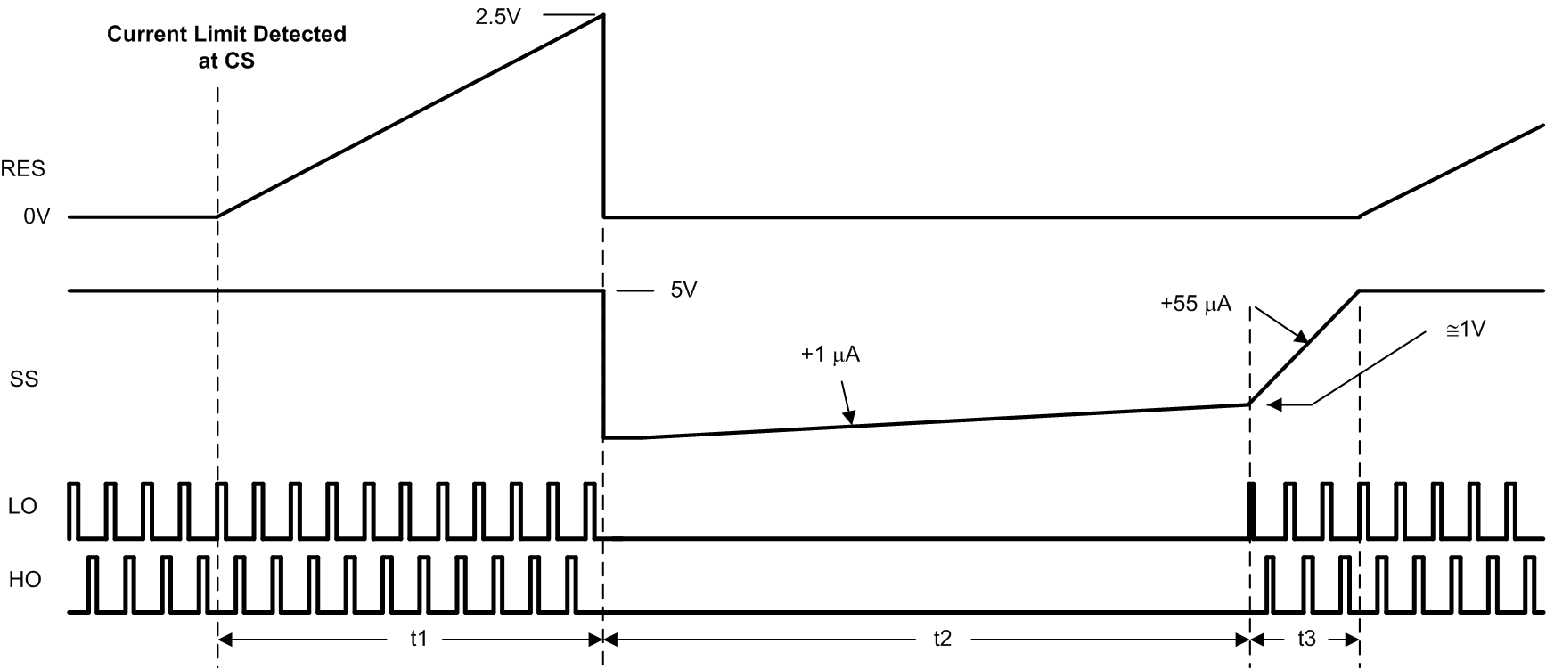 Figure 26. Hiccup Overload Restart Timing
In the case of continuous cycle-by-cycle current-limit detection at the CS pin, refer to Figure 26 and use Equation 17 to calculate the time required for CRES to reach the 2.5-V hiccup mode threshold.

For example, if CRES = 0.01 µF the time, t1, is approximately 1.14 ms.
The cool down time, t2 is set by the soft-start capacitor (CSS) and the internal 1-µA SS current source. Use Equation 18 to calculate the value of t2.

If CSS = 0.01 µF, the value of t2 is ≊ 10 ms.
The soft-start time t3 is set by the internal 55-µA current source. Use Equation 19 to calculate the value of t3.

If CSS = 0.01 µF, the value of t3 is ≊ 730 µs.
The time t2 provides a periodic cool-down time for the power converter in the event of a sustained overload or short circuit. This off time results in lower average input current and lower power dissipation within the power components. It is recommended that the ratio of t2 / (t1 + t3) be in the range of 5 to 10 to take advantage of this feature.
If the application requires no delay from the first detection of a current limit condition to the onset of the hiccup mode (t1 = 0), the RES pin can be left open (no external capacitor). If it is desired to disable the hiccup mode entirely, the RES pin must be connected to ground (AGND).
8.2.3 Application Curves
Figure 29 shows typical output ripple seen across the output terminals (with standard 10-µF and 1-µF ceramic capacitors) for an input voltage of 48 V and a load of 30 A. This waveform is typical of most loads and input voltages.
Figure 30 and Figure 31 show the drain voltage of Q1 with a 5-A load. Figure 30 represents an input voltage of 36 V and Figure 29 represents an input voltage of 72 V.
Figure 32 shows the gate voltages of the synchronous rectifiers. The dead time provided by the 20-kΩ DLY resistor is difficult to see at this timescale.
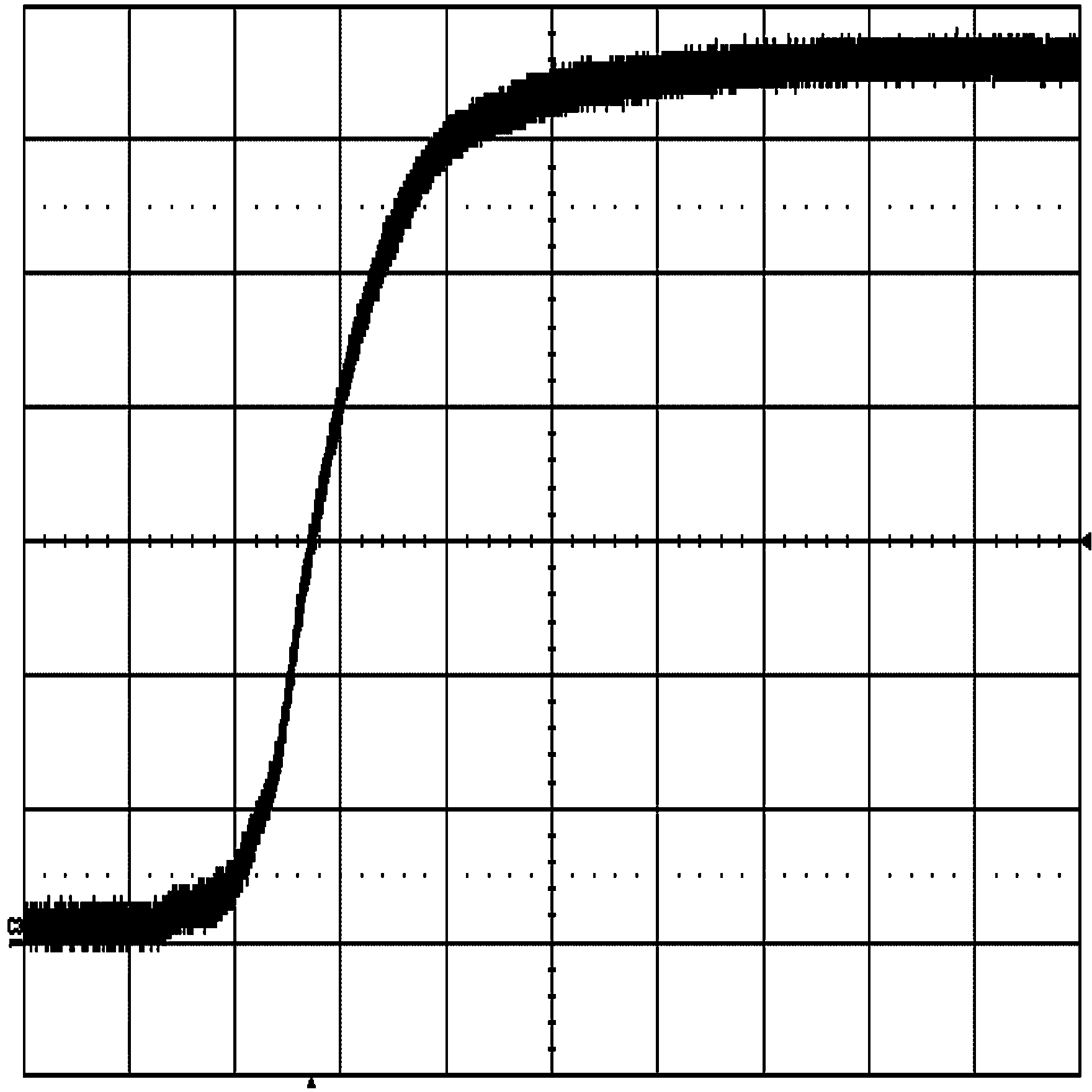
| VIN = 48 VDC | Horizontal resolution = 0.5 ms/div |
| IOUT = 5 A | Trace 1: output voltage V/div = 500 mV |
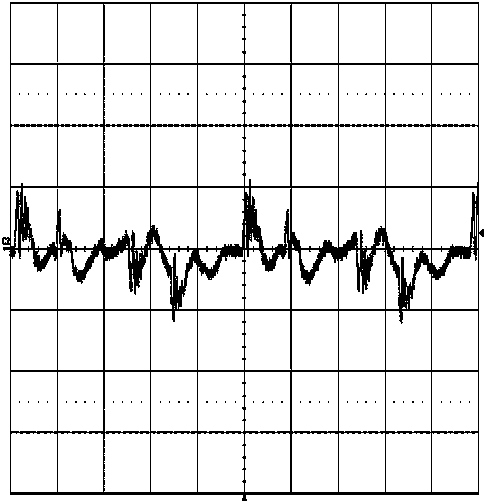
| VIN = 48 VDC | Trace 1: output ripple voltage V/div = 20 mV |
| IOUT = 30 A | Horizontal resolution = 1 µs/div |
| Bandwidth limit = 20 MHz |
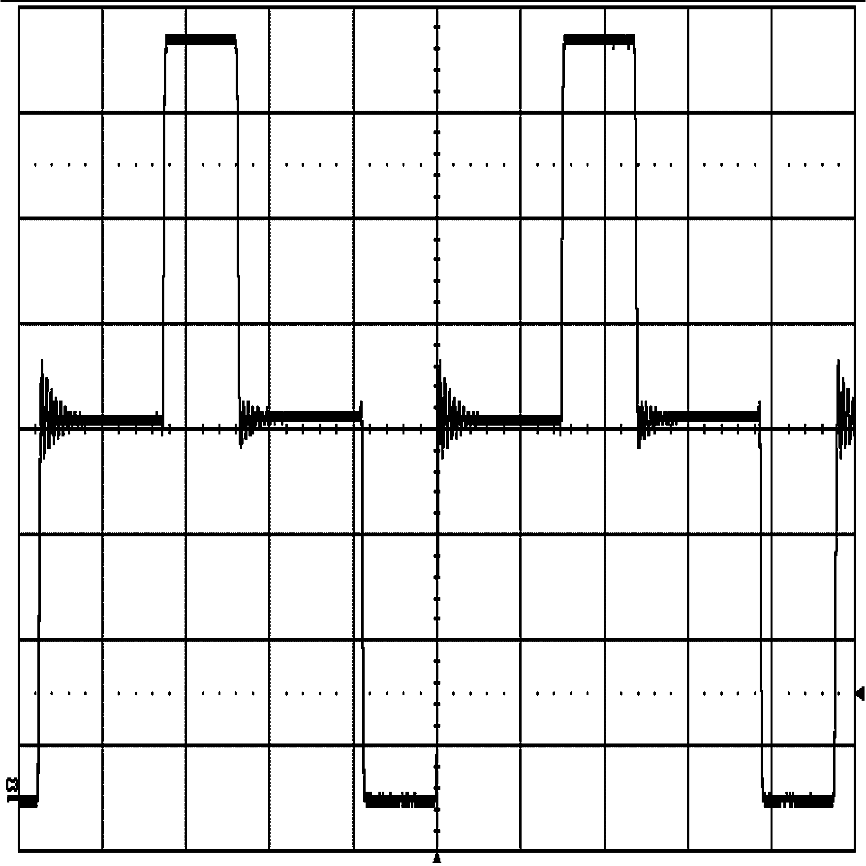
| VIN = 72 VDC | Trace 1: Q2 drain voltage V/div = 10 V |
| IOUT = 5 A | Horizontal resolution = 1 µs/div |
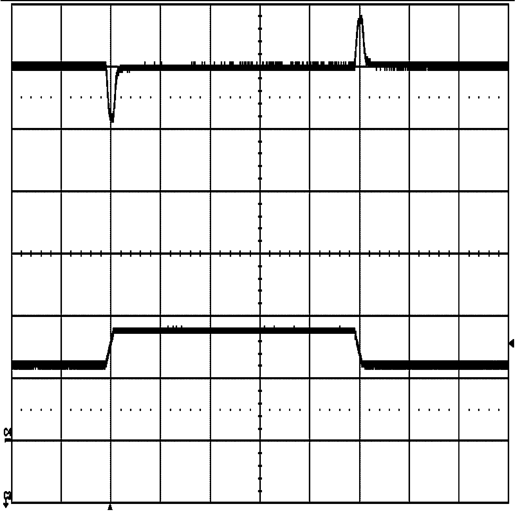
| VIN = 48 VDC | Horizontal resolution = 0.5 ms/div |
| IOUT = 15 A to 22.5 A | Upper trace: VOUT V/div = 50 mV |
| Lower trace: IOUT = 15 A to 22.5 A to 15 A | |
From 15 A to 22.5 A
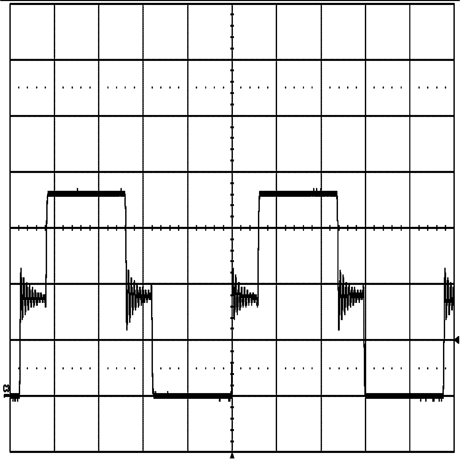
| VIN = 36 VDC | Trace 1: Q1 drain voltage V/div = 10 V |
| IOUT = 5 A | Horizontal resolution = 1 µs/div |
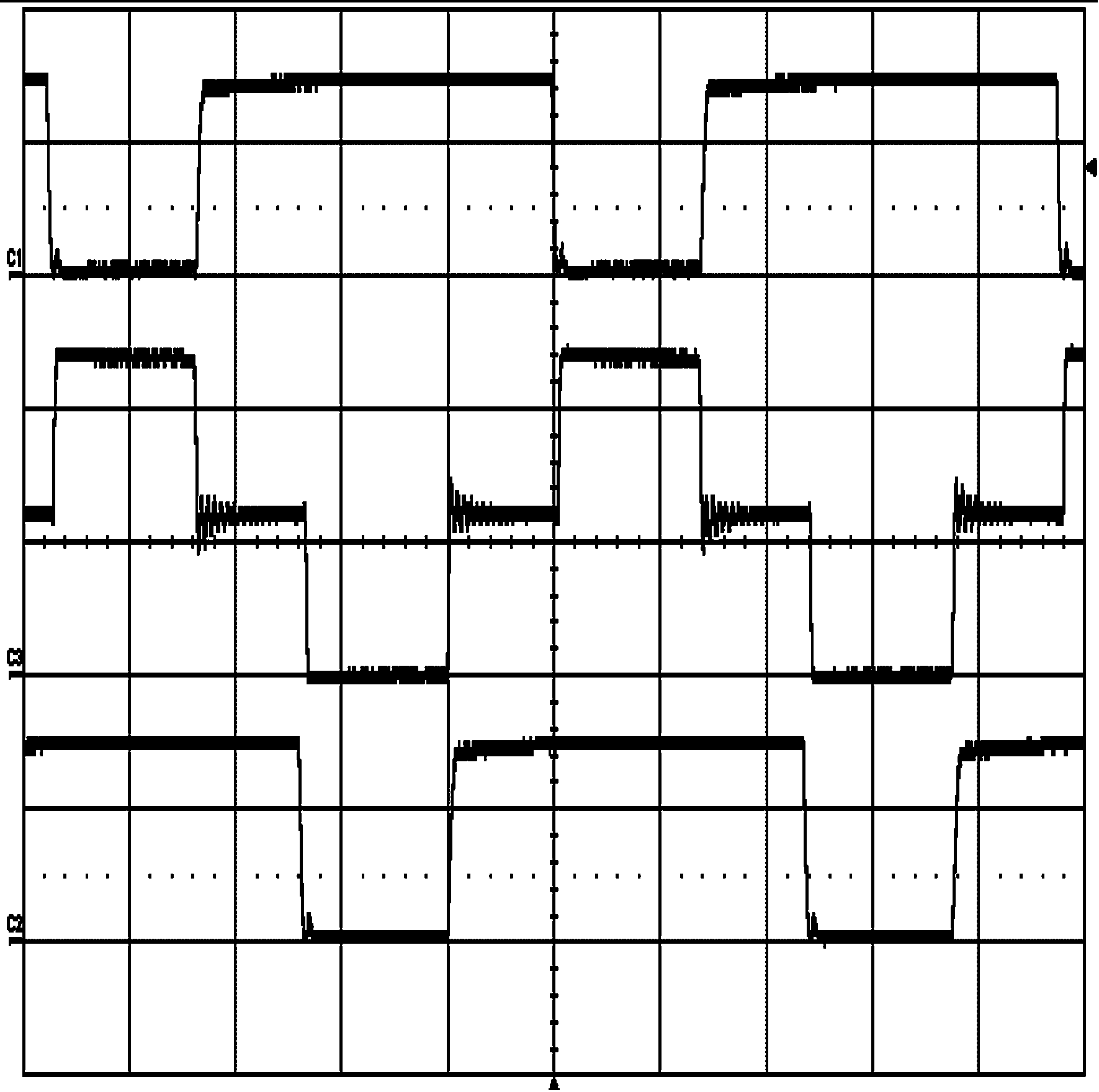
| VIN = 48 VDC | Upper trace: SR1, Q4 gate V/div = 5 V |
| IOUT = 5 A | Middle trace: HS, Q2 drain V/div = 20 V |
| Lower trace: SR2, Q6 gate V/div = 5 V | |
| Horizontal resolution = 1 µs/div |
