JAJSF12A March   2018  – January 2024 LMR14010A

PRODUCTION DATA  

  1.   1
  2. 特長
  3. アプリケーション
  4. 概要
  5. Pin Configuration and Functions
  6. Specifications
    1. 5.1 Absolute Maximum Ratings
    2. 5.2 ESD Ratings
    3. 5.3 Recommended Operating Conditions
    4. 5.4 Thermal Information
    5. 5.5 Electrical Characteristics
    6. 5.6 Typical Characteristics
  7. Detailed Description
    1. 6.1 Overview
    2. 6.2 Functional Block Diagram
    3. 6.3 Feature Description
      1. 6.3.1 Fixed Frequency PWM Control
      2. 6.3.2 Bootstrap Voltage (CB)
      3. 6.3.3 Setting the Output Voltage
      4. 6.3.4 Enable ( SHDN ) and VIN Undervoltage Lockout
      5. 6.3.5 Current Limit
      6. 6.3.6 Thermal Shutdown
    4. 6.4 Device Functional Modes
      1. 6.4.1 Continuous Conduction Mode
      2. 6.4.2 Eco-mode
  8. Application and Implementation
    1. 7.1 Application Information
    2. 7.2 Typical Application
      1. 7.2.1 Design Requirements
        1. 7.2.1.1 Step-By-Step Design Procedure
      2. 7.2.2 Detailed Design Procedure
        1. 7.2.2.1 Custom Design With WEBENCH® Tools
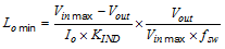
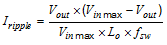
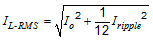
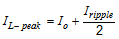
        2. 7.2.2.2 Output Inductor Selection
        3. 7.2.2.3 Output Capacitor Selection
        4. 7.2.2.4 Schottky Diode Selection
        5. 7.2.2.5 Input Capacitor Selection
        6. 7.2.2.6 Bootstrap Capacitor Selection
      3. 7.2.3 Application Performance Curves
    3. 7.3 Power Supply Recommendations
    4. 7.4 Layout
      1. 7.4.1 Layout Guidelines
      2. 7.4.2 Layout Example
  9. Device and Documentation Support
    1. 8.1 Device Support
      1. 8.1.1 Development Support
        1. 8.1.1.1 Custom Design With WEBENCH® Tools
    2. 8.2 ドキュメントの更新通知を受け取る方法
    3. 8.3 サポート・リソース
    4. 8.4 Trademarks
    5. 8.5 静電気放電に関する注意事項
    6. 8.6 用語集
  10. Revision History
  11. 10Mechanical, Packaging, and Orderable Information

パッケージ・オプション

メカニカル・データ(パッケージ|ピン)
サーマルパッド・メカニカル・データ
発注情報

Output Inductor Selection

The most critical parameters for the inductor are the inductance, peak current and the DC resistance. The inductance is related to the peak-to-peak inductor ripple current, the input and the output voltages. Because the ripple current increases with the input voltage, the maximum input voltage is always used to determine the inductance. Equation 1 is used to calculate the minimum value of the output inductor, where KIND is ripple current percentage. A reasonable value is setting the ripple current to be 30% (KIND) of the DC output current. For this design example, the minimum inductor value is calculated to be 16.4 µH, and a nearest standard value was chosen: 22 µH. For the output filter inductor, it is important that the RMS current and saturation current ratings not be exceeded. The RMS and peak inductor current can be found from Equation 3 and Equation 4. The inductor ripple current is 0.22 A, and the RMS current is 1 A. As the equation set demonstrates, lower ripple currents will reduce the output voltage ripple of the regulator but will require a larger value of inductance. A good starting point for most applications is 22 μH with a 1.6-A current rating. Using a rating near 1.6 A will enable the LMR14010A to current limit without saturating the inductor. This is preferable to the LMR14010A going into thermal shutdown mode and the possibility of damaging the inductor if the output is shorted to ground or other long-term overload.

Equation 1. GUID-1CC8087B-EF97-476D-9950-A055DDFEF1E8-low.gif
Equation 2. GUID-59312905-F7E5-407A-97A9-D8B75FD41E51-low.gif
Equation 3. GUID-1AA711B8-75FA-42B1-850F-301866AB9339-low.gif
Equation 4. GUID-903A2AC3-5704-41CD-BAC8-5B87474B899F-low.gif