JAJSEW0 March 2018 LMR23615-Q1
PRODUCTION DATA.
- 1 特長
- 2 アプリケーション
- 3 概要
- 4 改訂履歴
- 5 Pin Configuration and Functions
- 6 Specifications
-
7 Detailed Description
- 7.1 Overview
- 7.2 Functional Block Diagram
- 7.3
Feature Description
- 7.3.1 Fixed-Frequency Peak-Current-Mode Control
- 7.3.2 Adjustable Frequency
- 7.3.3 Adjustable Output Voltage
- 7.3.4 EN/SYNC
- 7.3.5 VCC, UVLO
- 7.3.6 Minimum ON-time, Minimum OFF-time and Frequency Foldback at Dropout Conditions
- 7.3.7 Internal Compensation and CFF
- 7.3.8 Bootstrap Voltage (BOOT)
- 7.3.9 Overcurrent and Short-Circuit Protection
- 7.3.10 Thermal Shutdown
- 7.4 Device Functional Modes
-
8 Application and Implementation
- 8.1 Application Information
- 8.2
Typical Applications
- 8.2.1 Design Requirements
- 8.2.2
Detailed Design Procedure
- 8.2.2.1 Custom Design With WEBENCH® Tools
- 8.2.2.2 Output Voltage Setpoint
- 8.2.2.3 Switching Frequency
- 8.2.2.4 Inductor Selection
- 8.2.2.5 Output Capacitor Selection
- 8.2.2.6 Feed-Forward Capacitor
- 8.2.2.7 Input Capacitor Selection
- 8.2.2.8 Bootstrap Capacitor Selection
- 8.2.2.9 VCC Capacitor Selection
- 8.2.2.10 Undervoltage Lockout Setpoint
- 8.2.3 Application Curves
- 9 Power Supply Recommendations
- 10Layout
- 11デバイスおよびドキュメントのサポート
- 12メカニカル、パッケージ、および注文情報
8.2 Typical Applications
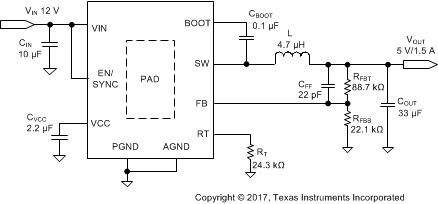
The LMR23615-Q1 only requires a few external components to convert from a wide voltage range supply to a fixed output voltage. Figure 22 shows a basic schematic.
 Figure 22. Application Circuit
The external components have to fulfill the needs of the application, but also the stability criteria of the device's control loop. Table 2 can be used to simplify the output filter component selection.
Table 2. L, COUT, and CFF Typical Values
| fSW (kHz) | VOUT (V) | L (µH) (1) | COUT (µF)(2) | CFF (pF)(3) | RFBT (kΩ)(4)(5) |
|---|---|---|---|---|---|
| 200 | 3.3 | 22 | 200 | 220 | 51 |
| 5 | 33 | 150 | 120 | 88.7 | |
| 12 | 56 | 68 | See note(3) | 243 | |
| 24 | 56 | 33 | See note(3) | 510 | |
| 400 | 3.3 | 10 | 120 | 100 | 51 |
| 5 | 15 | 90 | 68 | 88.7 | |
| 12 | 33 | 47 | See note(3) | 243 | |
| 24 | 33 | 22 | See note (3) | 510 | |
| 1000 | 3.3 | 4.7 | 68 | 47 | 51 |
| 5 | 5.6 | 47 | 22 | 88.7 | |
| 12 | 10 | 33 | See note(3) | 243 | |
| 2200 | 3.3 | 2.2 | 33 | 22 | 51 |
| 5 | 3.3 | 22 | 15 | 88.7 |
(1) Inductance value is calculated based on VIN = 36 V.
(2) All the COUT values are after derating. Add more when using ceramic capacitors.
(3) High ESR COUT will give enough phase boost and CFF not needed.
(4) RFBT = 0 Ω for VOUT = 1 V. RFBB = 22.1 kΩ for all other VOUT setting.
(5) For designs with RFBT other than recommended value, adjust CFF such that (CFF × RFBT) is unchanged and adjust RFBB such that (RFBT / RFBB) is unchanged.