JAJSHB8A May 2019 – October 2019 LMR34206-Q1
PRODUCTION DATA.
- 1 特長
- 2 アプリケーション
- 3 概要
- 4 改訂履歴
- 5 概要(続き)
- 6 Device Comparison Table
- 7 Pin Configuration and Functions
- 8 Specifications
- 9 Detailed Description
- 10Application and Implementation
- 11Power Supply Recommendations
- 12Layout
- 13デバイスおよびドキュメントのサポート
- 14メカニカル、パッケージ、および注文情報
9.4.1 Auto Mode
In auto mode the device moves between PWM and PFM as the load changes. At light loads the regulator operates in PFM. At higher loads the mode changes to PWM.
In PWM the regulator operates as a constant frequency, current mode, full synchronous converter using PWM to regulate the output voltage. While operating in this mode the output voltage is regulated by switching at a constant frequency and modulating the duty cycle to control the power to the load. This provides excellent line and load regulation and low output voltage ripple.
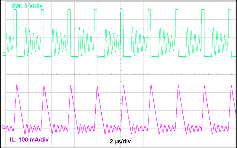
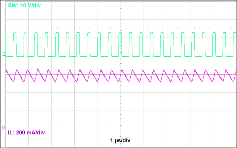
In PFM the high-side MOSFET is turned on in a burst of one or more pulses to provide energy to the load. The duration of the burst depends on how long it takes the inductor current to reach IPEAK-MIN. The frequency of these bursts is adjusted to regulate the output, while diode emulation (DEM) is used to maximize efficiency (see Glossary). This mode provides high light-load efficiency by reducing the amount of input supply current required to regulate the output voltage at small loads. This trades off very good light-load efficiency for larger output voltage ripple and variable switching frequency. Also, a small increase in output voltage occurs at light loads. The actual switching frequency and output voltage ripple depends on the input voltage, output voltage, and load. Typical switching waveforms in PFM and PWM are shown in Figure 13 and Figure 14.
 Figure 13. Typical PFM Switching Waveforms
VIN = 12 V, VOUT = 3.3 V, IOUT = 30 mA
 Figure 14. Typical PWM Switching Waveforms
VIN = 12 V, VOUT = 3.3 V, IOUT = 0.6 A, ƒS = 2100 kHz