JAJSHB8A May   2019  – October 2019 LMR34206-Q1

PRODUCTION DATA.  

  1. 特長
  2. アプリケーション
  3. 概要
    1.     Device Images
      1. 3.1 概略回路図
  4. 改訂履歴
  5. 概要(続き)
  6. Device Comparison Table
  7. Pin Configuration and Functions
    1.     Pin Functions
  8. Specifications
    1. 8.1 Absolute Maximum Ratings
    2. 8.2 ESD Ratings
    3. 8.3 Recommended Operating Conditions
    4. 8.4 Thermal Information
    5. 8.5 Electrical Characteristics
    6. 8.6 Timing Requirements
    7. 8.7 System Characteristics
    8. 8.8 Typical Characteristics
  9. Detailed Description
    1. 9.1 Overview
    2. 9.2 Functional Block Diagram
    3. 9.3 Feature Description
      1. 9.3.1 Power-Good Flag Output
      2. 9.3.2 Enable and Start-up
      3. 9.3.3 Current Limit and Short Circuit
      4. 9.3.4 Undervoltage Lockout and Thermal Shutdown
    4. 9.4 Device Functional Modes
      1. 9.4.1 Auto Mode
      2. 9.4.2 Forced PWM Operation
      3. 9.4.3 Dropout
      4. 9.4.4 Minimum Switch On-Time
      5. 9.4.5 Spread Spectrum Operation
  10. 10Application and Implementation
    1. 10.1 Application Information
    2. 10.2 Typical Application
      1. 10.2.1 Design Requirements
        1. 10.2.1.1 Design Requirements
      2. 10.2.2 Detailed Design Procedure
        1. 10.2.2.1 Choosing the Switching Frequency
        2. 10.2.2.2 Setting the Output Voltage
        3. 10.2.2.3 Inductor Selection
        4. 10.2.2.4 Output Capacitor Selection
        5. 10.2.2.5 Input Capacitor Selection
        6. 10.2.2.6 CBOOT
        7. 10.2.2.7 VCC
        8. 10.2.2.8 External UVLO
        9. 10.2.2.9 Maximum Ambient Temperature
      3. 10.2.3 Application Curves
  11. 11Power Supply Recommendations
  12. 12Layout
    1. 12.1 Layout Guidelines
      1. 12.1.1 Ground and Thermal Considerations
    2. 12.2 Layout Example
  13. 13デバイスおよびドキュメントのサポート
    1. 13.1 デバイス・サポート
      1. 13.1.1 開発サポート
    2. 13.2 ドキュメントのサポート
      1. 13.2.1 関連資料
    3. 13.3 ドキュメントの更新通知を受け取る方法
    4. 13.4 サポート・リソース
    5. 13.5 商標
    6. 13.6 静電気放電に関する注意事項
    7. 13.7 Glossary
  14. 14メカニカル、パッケージ、および注文情報

パッケージ・オプション

メカニカル・データ(パッケージ|ピン)
サーマルパッド・メカニカル・データ
発注情報

External UVLO

In some cases an input UVLO level different than that provided internal to the device is needed. This can be accomplished by using the circuit shown in Figure 19 can be used. The input voltage at which the device turns on is designated VON; while the turnoff voltage is VOFF. First a value for RENB is chosen in the range of 10 kΩ to 100 kΩ and then Equation 8 is used to calculate RENT and VOFF.

LMR34206-Q1 EN_uvlo_sch1.gifFigure 19. Set-up for External UVLO Application
Equation 8. LMR34206-Q1 EN_uvlo_eq1.gif
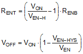
where

  • VON = VIN turnon voltage
  • VOFF = VIN turnoff voltage