JAJSG01D June 2012 – August 2018 LMZ20502
PRODUCTION DATA.
- 1 特長
- 2 アプリケーション
- 3 概要
- 4 改訂履歴
- 5 Pin Configuration and Functions
- 6 Specifications
- 7 Detailed Description
- 8 Application and Implementation
- 9 Power Supply Recommendations
- 10Layout
- 11デバイスおよびドキュメントのサポート
- 12メカニカル、パッケージ、および注文情報
パッケージ・オプション
デバイスごとのパッケージ図は、PDF版データシートをご参照ください。
メカニカル・データ(パッケージ|ピン)
- SIL|8
サーマルパッド・メカニカル・データ
発注情報
10.3 Soldering Information
Proper operation of the LMZ20502 requires that it be correctly soldered to the PCB. This is especially true regarding the EP. This pad acts as a quiet ground reference for the device and a heatsink connection. Use the following recommendations when utilizing machine placement of the device:
- Dimension of area for pick-up: 2 mm x 2.5 mm.
- Use a nozzle size of less than 1.3 mm in diameter, so that the head does not touch the outer area of the package.
- Use a soft tip pick-and-place head.
- Add 0.05 mm to the component thickness so that the device will be released 0.05 mm into the solder paste without putting pressure or splashing the solder paste.
- Slow the pick arm when picking the part from the tape and reel carrier and when depositing the device on the board.
- If the machine releases the component by force, use the minimum force and no more than 3 N.
- For PCBs with surface mount components on both sides, it is suggested to put the LMZ20502 on the top side. In case the application requires bottom side placement, a re-flow fixture may be required to protect the module during the second reflow.
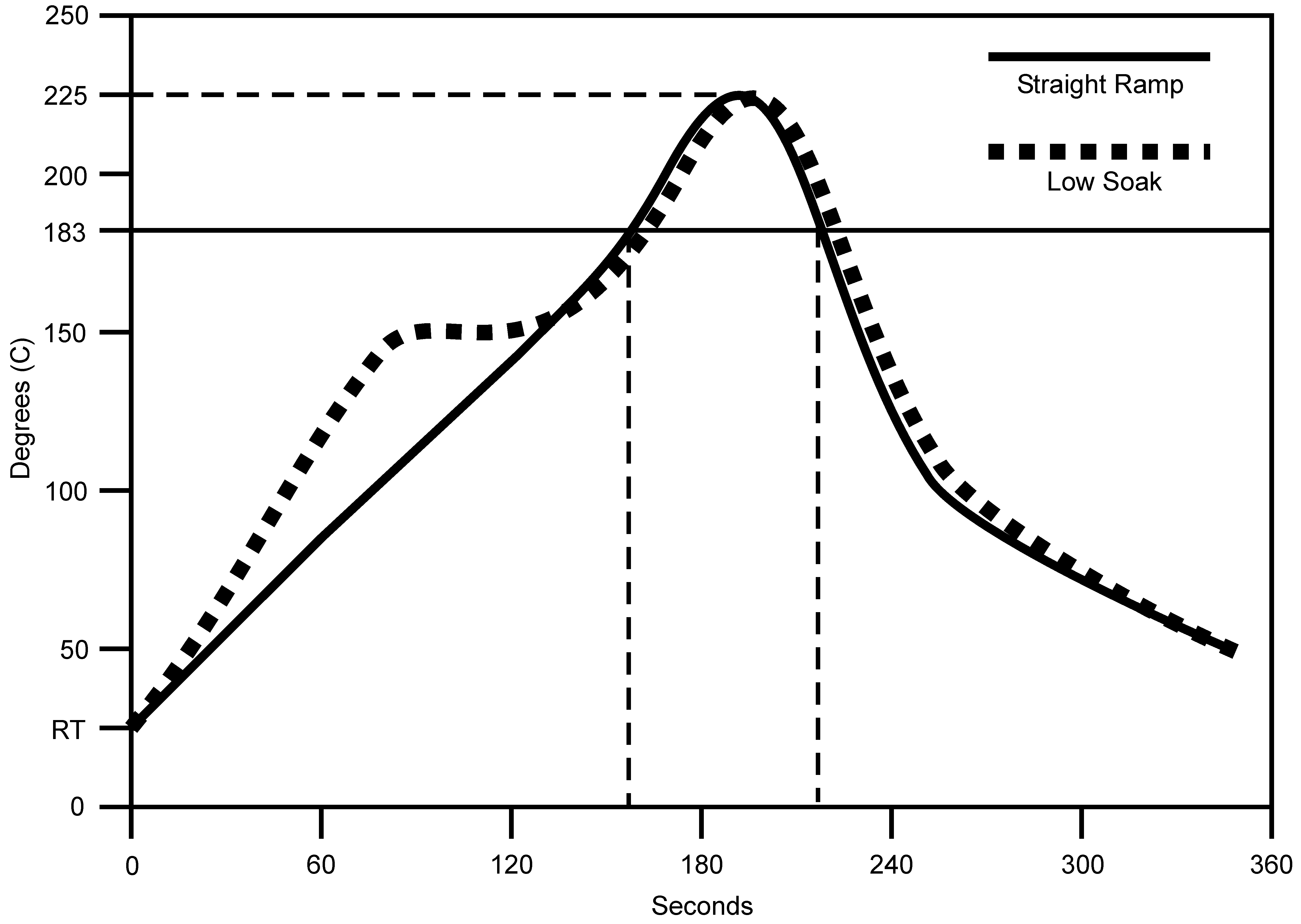
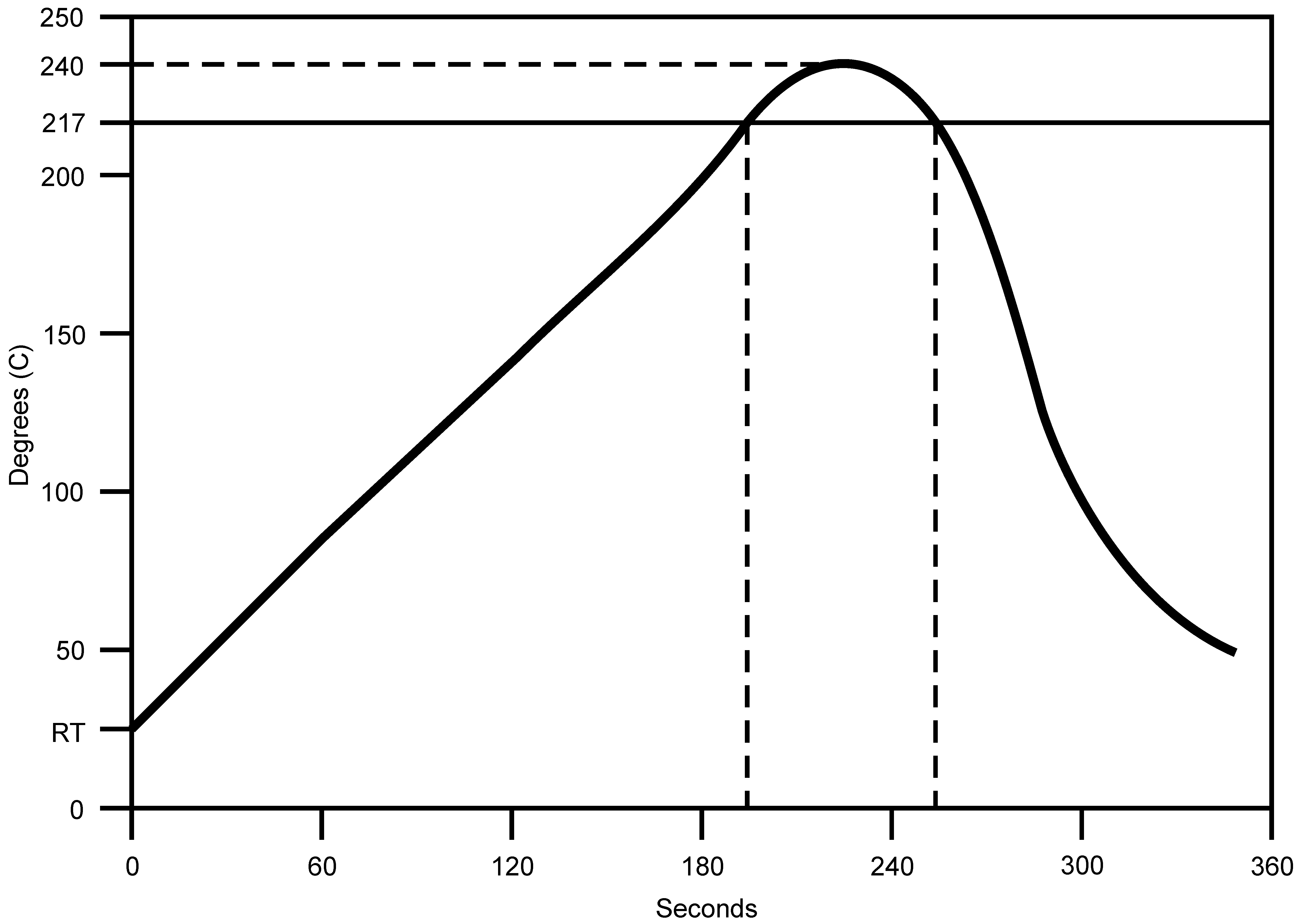
In addition, please follow the important guidelines found in: SNOA401. The curves in Figure 40 and Figure 41 show typical soldering temperature profiles.
 Figure 40. Typical Re-flow Profile Eutectic (63sn/37pb) Solder Paste
 Figure 41. Typical Re-flow Profile Lead-Free (Sca305 Or Sac405) Solder Paste