JAJSCR1 November 2016 LP5922
PRODUCTION DATA.
- 1 特長
- 2 アプリケーション
- 3 概要
- 4 改訂履歴
- 5 Pin Configuration and Functions
- 6 Specifications
- 7 Detailed Description
-
8 Applications and Implementation
- 8.1 Application Information
- 8.2
Typical Application
- 8.2.1 Design Requirements
- 8.2.2
Detailed Design Procedure
- 8.2.2.1 External Capacitors
- 8.2.2.2 Input Capacitor, CIN
- 8.2.2.3 Output Capacitor, COUT
- 8.2.2.4 Soft-Start and Noise-Reduction Capacitor, CSS/NR
- 8.2.2.5 Feed-Forward Capacitor, CFF
- 8.2.2.6 No-Load Stability
- 8.2.2.7 Power Dissipation
- 8.2.2.8 Estimating Junction Temperature
- 8.2.2.9 Recommended Continuous Operating Area
- 8.2.3 Application Curves
- 9 Power Supply Recommendations
- 10Layout
- 11デバイスおよびドキュメントのサポート
- 12メカニカル、パッケージ、および注文情報
6 Specifications
6.1 Absolute Maximum Ratings
over operating free-air temperature range (unless otherwise noted)(1)(2)| MIN | MAX | UNIT | ||
|---|---|---|---|---|
| IN pin voltage, VIN | –0.3 | 7 | V | |
| OUT pin voltage, VOUT | See(3) | |||
| EN pin voltage, VEN | –0.3 | 7 | V | |
| PG pin voltage, VPG | –0.3 | 7 | V | |
| SS/NR pin voltage, VSS/NR | –0.3 | 3.6 | V | |
| FB pin voltage, VFB | –0.3 | 3.6 | V | |
| Junction temperature, TJ | 150 | °C | ||
| Continuous power dissipation(4) | Internally limited | |||
| Storage temperature, Tstg | –65 | 150 | °C | |
(1) Stresses beyond those listed under Absolute Maximum Ratings may cause permanent damage to the device. These are stress ratings only, which do not imply functional operation of the device at these or any other conditions beyond those indicated under Recommended Operating Conditions. Exposure to absolute-maximum-rated conditions for extended periods may affect device reliability.
(2) All voltages are with respect to the potential at the GND pin.
(3) Absolute maximum VOUT is the lesser of VIN + 0.3 V, or 7 V.
(4) Internal thermal shutdown circuitry protects the device from permanent damage.
6.2 ESD Ratings
| VALUE | UNIT | |||
|---|---|---|---|---|
| V(ESD) | Electrostatic discharge | Human-body model (HBM), per ANSI/ESDA/JEDEC JS-001(1) | ±2000 | V |
| Charged-device model (CDM), per JEDEC specification JESD22-C101(2) | ±1000 | |||
(1) JEDEC document JEP155 states that 500-V HBM allows safe manufacturing with a standard ESD control process
(2) JEDEC document JEP157 states that 250-V CDM allows safe manufacturing with a standard ESD control process.
6.3 Recommended Operating Conditions
over operating free-air temperature range (unless otherwise noted)| MIN | NOM | MAX | UNIT | ||
|---|---|---|---|---|---|
| Input voltage, VIN | 1.3 | 6 | V | ||
| Output voltage, VOUT | 0.5 | 5 | V | ||
| FB voltage, VFB | 0.5 | V | |||
| EN input voltage, VEN | 0 | VIN | V | ||
| Recommended load current, IL | 0 | 2 | A | ||
| Operating junction temperature, TJ-MAX-OP | –40 | 125 | °C | ||
6.4 Thermal Information
| THERMAL METRIC(1) | LP5922 | UNIT | |
|---|---|---|---|
| DSC (WSON) | |||
| 10 PINS | |||
| RθJA(2) | Junction-to-ambient thermal resistance, High K | 49.5(3) | °C/W |
| RθJC(top) | Junction-to-case (top) thermal resistance | 38.2 | °C/W |
| RθJB | Junction-to-board thermal resistance | 24.0 | °C/W |
| ψJT | Junction-to-top characterization parameter | 0.5 | °C/W |
| ψJB | Junction-to-board characterization parameter | 24.1 | °C/W |
| RθJC(bot) | Junction-to-case (bottom) thermal resistance | 6.0 | °C/W |
(1) For more information about traditional and new thermal metrics, see Semiconductor and IC Package Thermal Metrics.
(2) Thermal resistance value RθJA is based on the EIA/JEDEC High-K printed circuit board defined by JESD51-7 - High Effective Thermal Conductivity Test Board for Leaded Surface Mount Packages.
(3) The PCB for the WSON/DSC package RθJA includes four (4) thermal vias, in a 2 × 2 array, under the exposed thermal pad per EIA/JEDEC JESD51-5.
6.5 Electrical Characteristics
VIN = VOUT(NOM) + 0.5 V or 1.3 V, whichever is greater; VEN = 1.2 V, CIN = 22 μF, COUT = 22 μF, OUT connected to 50 Ω to GND, VFB = 0.5 V, CSS/NR = 0.12 µF, CFF = 0.01 µF, and PG pin pulled up to VIN by 100-kΩ resistor (unless otherwise noted).(1)(2)(3)| PARAMETER | TEST CONDITIONS | MIN | TYP | MAX | UNIT | |
|---|---|---|---|---|---|---|
| SUPPLY VOLTAGE | ||||||
| VIN | Input voltage range | 1.3 | 6 | V | ||
| UVLO | Undervoltage lock-out threshold | VIN Rising (↑) until output is ON | 1.2 | 1.25 | V | |
| ΔUVLO | UVLO hysteresis | VIN Falling (↓) from UVLO threshold until output is OFF | 160 | mV | ||
| OUTPUT VOLTAGE AND REGULATION | ||||||
| VOUT | Output voltage range | 0.5 | 5 | V | ||
| ΔVOUT | Line regulation | IOUT = 5 mA, 1.3 V ≤ VIN ≤ 6 V | 0.02 | %/V | ||
| Load regulation | 5 mA ≤ IOUT ≤ 2 A | 0.1 | %/A | |||
| VDO | Dropout voltage(4) | VIN = 1.4 V, IOUT = 2 A | 220 | 400 | mV | |
| VIN = 2.5 V, IOUT = 2 A | 100 | 180 | ||||
| VIN = 5.3 V, IOUT = 2 A | 90 | 160 | ||||
| FB | ||||||
| VFB | FB voltage | IOUT = 5 mA to 2 A | 492.5 | 500 | 507.5 | mV |
| IFB | FB pin input current | VFB = 0.5 V | –100 | 100 | nA | |
| CURRENT LEVELS | ||||||
| IL | Maximum load current | VIN ≥ 1.3 V | 2 | A | ||
| ISC | Short-circuit current limit(5) | 2.2 | 3 | 3.8 | A | |
| IGND | Ground-current minimum load(7) | VIN = 6 V, IOUT = 0 mA | 0.7 | mA | ||
| Ground-current maximum load(7) | VIN = 1.3 V, IOUT = 2 A | 1 | 4 | |||
| IGND(SD) | Shutdown current(6) | VIN = 6 V, VEN = 0 V, VPG = 0 V | 0.1 | 15 | µA | |
| VIN to VOUT RIPPLE REJECTION (9) | ||||||
| PSRR | Power-supply rejection ratio | VIN ≥ 1.4 V, ƒ = 1 kHz, IOUT = 2 A | 70 | dB | ||
| VIN ≥ 1.4 V, ƒ = 10 kHz, IOUT = 2 A | 55 | |||||
| VIN ≥ 1.4 V, ƒ = 100 kHz, IOUT = 2 A | 40 | |||||
| VIN ≥ 1.4 V, ƒ = 1 MHz, IOUT = 2 A | 30 | |||||
| OUTPUT NOISE VOLTAGE | ||||||
| eN | Noise voltage(9) | VIN= 2.5 V, VOUT= 1.8 V BW = 10 Hz to 100 kHz |
25 | µVRMS | ||
| LOGIC INPUT THRESHOLDS | ||||||
| VIL(EN) | EN pin low threshold | VEN falling (↓) until output is OFF | 0.35 | V | ||
| VIH(EN) | EN pin high threshold | VEN rising (↑) until output is ON | 1.2 | V | ||
| IEN | Input current at EN pin (8) | VIN = 6 V, VEN = 6 V | 3 | µA | ||
| PGHTH | PG high threshold (% of nominal VOUT) | VOUT rising (↑) until PG goes high | 94% | |||
| PGLTH | PG low threshold (% of nominal VOUT) | VOUT falling (↓) until PG goes low | 90% | |||
| VOL(PG) | PG pin low-level output voltage | VOUT < PGLTH, sink current = 1 mA | 400 | mV | ||
| ILKG(PG) | PG pin leakage current | VOUT > PGHTH, VPG = 6 V | 1 | µA | ||
| SOFT START | ||||||
| ISS | SS/NR pin charging current | 6.2 | µA | |||
| THERMAL SHUTDOWN | ||||||
| TSD | Thermal shutdown temperature | 165 | °C | |||
| ΔTSD | Thermal shutdown hysteresis | 15 | °C | |||
| TRANSITION CHARACTERISTICS | ||||||
| ΔVOUT | Line transients | ΔVIN = 0.5 V, VOUT = 2.8 V, tRISE = tFALL = 5 μs |
3 | mV | ||
| Load transients | VOUT = 3.3 V, IOUT = 10 mA to 2 A to 10 mA tRISE = tFALL = 1 V/μs |
25 | ||||
| RAD | Output discharge pull-down resistance | VEN = 0 V, VIN = 2.3 V | 400 | Ω | ||
(1) All voltages are with respect to the GND pin.
(2) Minimum and maximum limits are design targeted limits over the junction temperature (TJ) range of –40°C to +125°C, unless otherwise stated. Typical values represent the most likely parametric norm at TJ = 25°C, and are provided for reference purposes only.
(3) CIN, COUT: Low-ESR surface-mount-ceramic capacitors (MLCCs) used in setting electrical characteristics.
(4) Dropout voltage is the voltage difference between the input and the output at which the FB voltage drops to 97% of its nominal value.
(5) Short-circuit current (ISC) is equivalent to current limit. To minimize thermal effects during testing, ISC is measured with VOUT pulled to 100 mV below its nominal voltage.
(6) Ground current in shutdown mode, IGND(SD), does NOT include current from PG pin.
(7) Ground current is defined here as the total current flowing to ground as a result of all voltages applied to the device
IGND = ( (IIN – IOUT) + IEN + ILKG(PG))
IGND = ( (IIN – IOUT) + IEN + ILKG(PG))
(8) There is a 2-MΩ resistor between EN and ground (pulldown) on the device.
(9) This specification is verified by design.
6.6 Input and Output Capacitors
over operating free-air temperature range (unless otherwise noted)| PARAMETER | TEST CONDITIONS | MIN | TYP | MAX | UNIT | |
|---|---|---|---|---|---|---|
| CIN | Input capacitance(1) | 22 | µF | |||
| COUT | Output capacitance | VOUT ≤ 0.8 V | 34 | 47 | µF | |
| VOUT > 0.8 V | 15 | 22 | ||||
(1) Typically input capacitance placed close to the device is in the same order as output capacitance. See also Input Capacitor, CIN.
6.7 Typical Characteristics
VIN = VOUT + 0.5 V, VEN = 1.2 V, CIN = 22 μF, COUT = 22 μF, OUT connected to 50 Ω to GND, VFB = 0.5 V, CSS/NR = 0.12 µF, CFF = 0.01 µF, and PG pin pulled up to VIN by 100-kΩ resistor and TJ = 25°C, unless otherwise stated.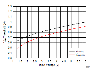
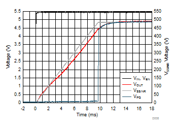
| VOUT = 5 V | VEN = VIN | IOUT = 1 mA |
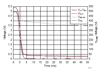
| VOUT = 5 V | VEN = VIN | IOUT = 1 mA |
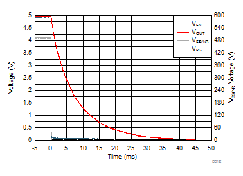
| VOUT = 5 V | IOUT = 1 mA |
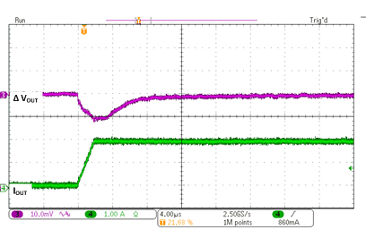
| VOUT = 2.8 V | IOUT = 10 mA to 2 A | trise = 1 V/µs |
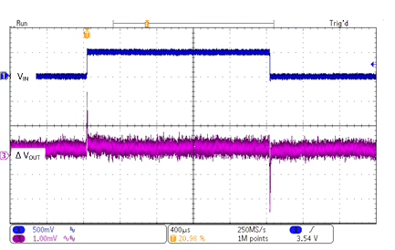
| VOUT = 2.8 V | VIN 3.3 V to 3.8V to 3.3 V | tfall = 1 V/µs |
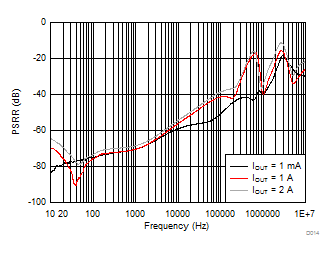
| VIN = 5.5 V | VOUT = 5 V |
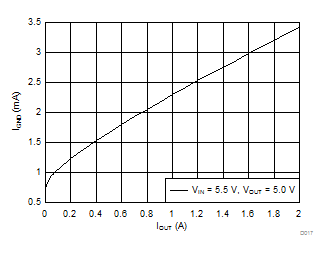
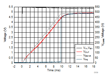
| VOUT = 5 V | VEN = VIN | IOUT = 2 A |
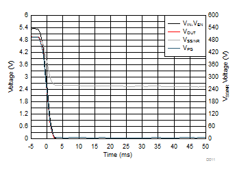
| VOUT = 5 V | VEN = VIN | IOUT = 2 A |
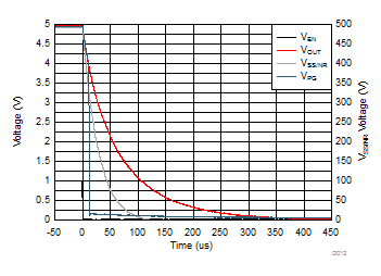
| VOUT = 5 V | IOUT = 2 A |

| VOUT = 2.8 V | IOUT = 2 A to 10 mA | tfall = 1 V/µs |
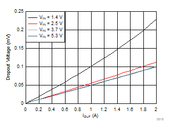
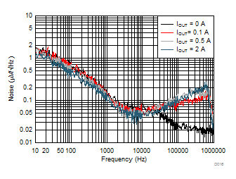
| VIN = 2.5 V | VOUT = 1.8 V |