JAJSEA5D December 2017 – October 2019 OPA207
PRODUCTION DATA.
- 1 特長
- 2 アプリケーション
- 3 概要
- 4 改訂履歴
- 5 Pin Configuration and Functions
- 6 Specifications
- 7 Detailed Description
- 8 Application and Implementation
- 9 Power Supply Recommendations
- 10Layout
- 11デバイスおよびドキュメントのサポート
- 12メカニカル、パッケージ、および注文情報
パッケージ・オプション
メカニカル・データ(パッケージ|ピン)
サーマルパッド・メカニカル・データ
発注情報
7.3.6 Low Input Bias Current
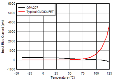
The OPA207 uses super-beta bipolar transistors and employs an input bias current cancellation technique. This combination results in very low input bias currents that remain low over the full specified temperature range from –40°C to + 125°C unlike CMOS or JFET amplifiers whose input bias currents typically double every 10°C and can be extremely high at 125°C. Figure 43 illustrates the comparison between the OPA207 and typical CMOS or JFET amplifiers.
 Figure 43. Input Bias Current vs Temperature
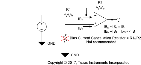
 It is common practice to place a bias current cancellation resistor as illustrated in Figure 42. This approach works well with amplifiers that do not employ an internal input bias current cancellation technique. Because the OPA207 uses an internal bias current cancellation technique, TI does not recommend the bias cancellation resistor.
 Figure 44. Bias Current Cancellation Resistor — Not Recommended