JAJSDR3D September 2017 – December 2018 OPA2837 , OPA837
PRODUCTION DATA.
- 1 特長
- 2 アプリケーション
- 3 概要
- 4 改訂履歴
- 5 Pin Configuration and Functions
-
6 Specifications
- 6.1 Absolute Maximum Ratings
- 6.2 ESD Ratings
- 6.3 Recommended Operating Conditions
- 6.4 Thermal Information: OPA837
- 6.5 Thermal Information: OPA2837
- 6.6 Electrical Characteristics: VS = 5 V
- 6.7 Electrical Characteristics: VS = 3 V
- 6.8 Typical Characteristics: VS = 5.0 V
- 6.9 Typical Characteristics: VS = 3.0 V
- 6.10 Typical Characteristics: ±2.5-V to ±1.5-V Split Supply
- 7 Detailed Description
-
8 Application and Implementation
- 8.1
Application Information
- 8.1.1 Noninverting Amplifier
- 8.1.2 Inverting Amplifier
- 8.1.3 Output DC Error Calculations
- 8.1.4 Output Noise Calculations
- 8.1.5 Instrumentation Amplifier
- 8.1.6 Attenuators
- 8.1.7 Differential to Single-Ended Amplifier
- 8.1.8 Differential-to-Differential Amplifier
- 8.1.9 Pulse Application With Single-Supply Circuit
- 8.1.10 ADC Driver Performance
- 8.2 Typical Applications
- 8.1
Application Information
- 9 Power Supply Recommendations
- 10Layout
- 11デバイスおよびドキュメントのサポート
- 12メカニカル、パッケージ、および注文情報
パッケージ・オプション
メカニカル・データ(パッケージ|ピン)
サーマルパッド・メカニカル・データ
発注情報
8.2.3 1-Bit PGA Operation
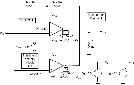
Using the internal inverting input switch that operates along with the power disable function can also allow a simple gain selection on a single input signal. Figure 88 shows an example gain select of either 1 V/V or 2 V/V from a single input to a single output. The logic disables both channels before turning one of them on to avoid high currents in both outputs to be active at the same time. If this approach is not possible, as in the simple switch shown in Figure 88, insert 100-Ω resistors inside the loop of each op amp output. A bipolar supply is shown in Figure 88, but any of the single-supply options are also possible. Any combination of gains can be implemented, but wide gain ranges show a larger change in signal bandwidth. This approach can be expanded to more than two gain settings. Testing with the circuit of Figure 88 showed no change in harmonic distortion; see Figure 18 and Figure 36.
 Figure 88. 1-Bit PGA