JAJSFO1G September   2012  – June 2018 SN65DSI84

PRODUCTION DATA.  

  1. 特長
  2. アプリケーション
  3. 概要
    1.     標準アプリケーション
  4. 改訂履歴
  5. Pin Configuration and Functions
    1.     Pin Functions
  6. Specifications
    1. 6.1 Absolute Maximum Ratings
    2. 6.2 EDS Ratings
    3. 6.3 Recommended Operating Conditions
    4. 6.4 Thermal Information
    5. 6.5 Electrical Characteristics
    6. 6.6 Switching Characteristics
  7. Detailed Description
    1. 7.1 Overview
    2. 7.2 Functional Block Diagram
    3. 7.3 Feature Description
      1. 7.3.1 Clock Configurations and Multipliers
      2. 7.3.2 ULPS
      3. 7.3.3 LVDS Pattern Generation
    4. 7.4 Device Functional Modes
      1. 7.4.1 Reset Implementation
      2. 7.4.2 Initialization Sequence
      3. 7.4.3 LVDS Output Formats
      4. 7.4.4 DSI Lane Merging
      5. 7.4.5 DSI Pixel Stream Packets
      6. 7.4.6 DSI Video Transmission Specifications
      7. 7.4.7 Operating Modes
    5. 7.5 Programming
      1. 7.5.1 Local I2C Interface Overview
    6. 7.6 Register Maps
      1. 7.6.1 Control and Status Registers Overview
  8. Application and Implementation
    1. 8.1 Application Information
      1. 8.1.1 Video Stop and Restart Sequence
      2. 8.1.2 Reverse LVDS Pin Order Option
      3. 8.1.3 IRQ Usage
    2. 8.2 Typical Application
      1. 8.2.1 Design Requirements
      2. 8.2.2 Detailed Design Procedure
        1. 8.2.2.1 Example Script
      3. 8.2.3 Application Curve
  9. Power Supply Recommendations
    1. 9.1 VCC Power Supply
    2. 9.2 VCORE Power Supply
  10. 10Layout
    1. 10.1 Layout Guidelines
      1. 10.1.1 Package Specific
      2. 10.1.2 Differential Pairs
      3. 10.1.3 Ground
    2. 10.2 Layout Example
  11. 11デバイスおよびドキュメントのサポート
    1. 11.1 ドキュメントの更新通知を受け取る方法
    2. 11.2 コミュニティ・リソース
    3. 11.3 商標
    4. 11.4 静電気放電に関する注意事項
    5. 11.5 Glossary
  12. 12メカニカル、パッケージ、および注文情報

パッケージ・オプション

メカニカル・データ(パッケージ|ピン)
サーマルパッド・メカニカル・データ
発注情報

DSI Lane Merging

The SN65DSI84 supports four DSI data lanes per input channel, and may be configured to support one, two, or three DSI data lanes per channel. Unused DSI input pins on the SN65DSI84 should be left unconnected or driven to LP11 state. The bytes received from the data lanes are merged in HS mode to form packets that carry the video stream. DSI data lanes are bit and byte aligned.

Figure 13 illustrates the lane merging function for each channel; 4-Lane, 3-Lane, and 2-Lane modes are illustrated
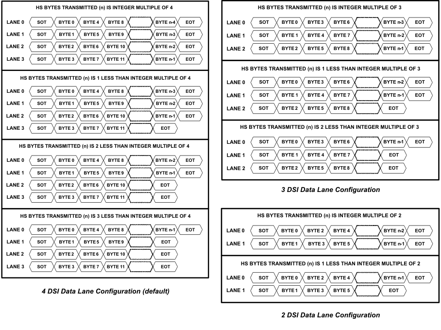
SN65DSI84 lane_merging_LLSEB9.gifFigure 13. SN65DSI84 DSI Lane Merging Illustration