SLLSEH0F July 2013 – August 2014 SN65HVD01
PRODUCTION DATA.
- 1 Features
- 2 Applications
- 3 Description
- 4 Revision History
- 5 Pin Configuration and Functions
- 6 Specifications
- 7 Parameter Measurement Information
- 8 Detailed Description
- 9 Applications and Implementation
- 10Power Supply Recommendations
- 11Layout
- 12Device and Documentation Support
- 13Mechanical, Packaging, and Orderable Information
パッケージ・オプション
メカニカル・データ(パッケージ|ピン)
- DRC|10
サーマルパッド・メカニカル・データ
- DRC|10
発注情報
7 Parameter Measurement Information
Input generator rate is 100 kbps, 50% duty cycle, rise and fall times less than 6 nsec.
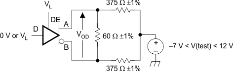 Figure 9. Measurement of Driver Differential Output Voltage with Common-Mode Load
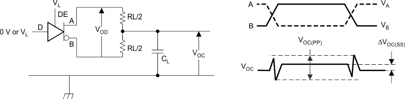 Figure 10. Measurement of Driver Differential and Common-Mode Output with RS-485 Load
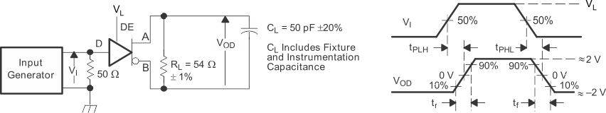 Figure 11. Measurement of Driver Differential Output Rise and Fall Times and Propagation Delays
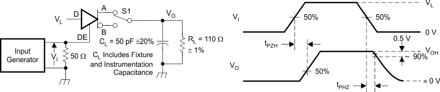
D at VL to test non-inverting output, D at 0 V to test inverting output.
Figure 12. Measurement of Driver Enable and Disable Times with Active High Output and Pull-Down Load
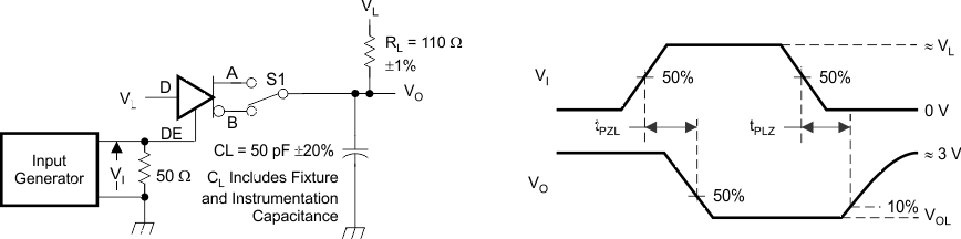
D at 0V to test non-inverting output, D at VL to test inverting output.
Figure 13. Measurement of Driver Enable and Disable Times with Active Low Output and Pull-Up Load
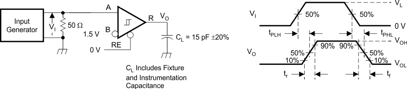 Figure 14. Measurement of Receiver Output Rise and Fall Times and Propagation Delays
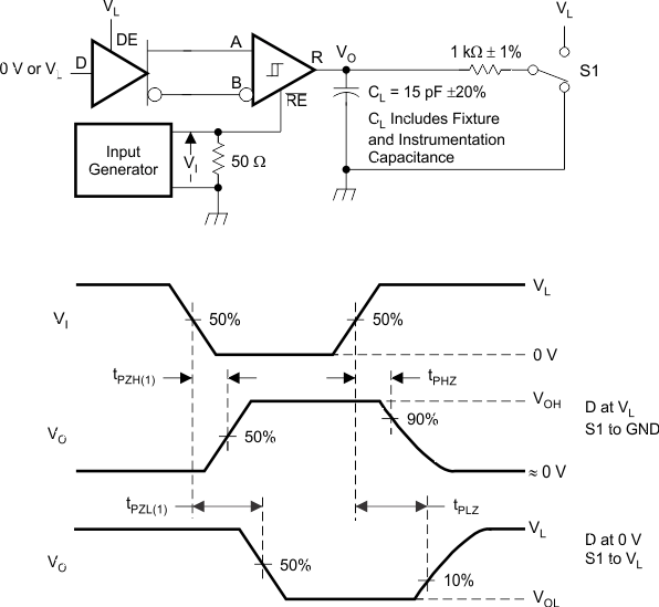 Figure 15. Measurement of Receiver Enable/Disable Times with Driver Enabled
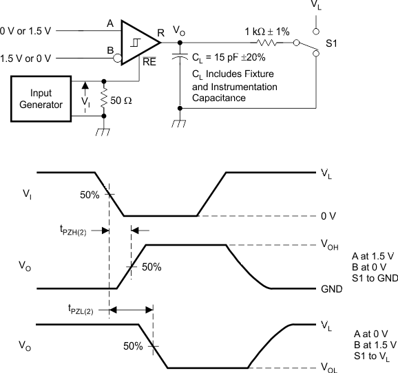 Figure 16. Measurement of Receiver Enable Times with Driver Disabled