SLLSEH0F July 2013 – August 2014 SN65HVD01
PRODUCTION DATA.
- 1 Features
- 2 Applications
- 3 Description
- 4 Revision History
- 5 Pin Configuration and Functions
- 6 Specifications
- 7 Parameter Measurement Information
- 8 Detailed Description
- 9 Applications and Implementation
- 10Power Supply Recommendations
- 11Layout
- 12Device and Documentation Support
- 13Mechanical, Packaging, and Orderable Information
パッケージ・オプション
メカニカル・データ(パッケージ|ピン)
- DRC|10
サーマルパッド・メカニカル・データ
- DRC|10
発注情報
5 Pin Configuration and Functions
DRC 10 PIN
(TOP VIEW)
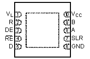
Pin Functions
| NAME | NO. | I/O | DESCRIPTION |
|---|---|---|---|
| VL | 1 | Logic Supply | 1.65 V to 3.6 V supply for logic I/O signals R, RE, D, DE, and SLR) |
| R | 2 | Digital Output | Receive data output |
| DE | 3 | Digital Input | Driver enable input |
| RE | 4 | Digital Input | Receiver enable input |
| D | 5 | Digital Input | Transmission data input |
| GND | 6 | Reference Potential | Local device ground |
| SLR | 7 | Digital Input | Slew rate select: Low = 20 Mbps, High = 250 kbps. Defaults to 20 Mbps if SLR is left floating |
| A | 8 | Bus I/O | Digital bus I/O, A |
| B | 9 | Bus I/O | Digital bus I/O, B |
| VCC | 10 | Bus Supply | 3 V to 3.6 V supply for A and B bus lines |