JAJSF09B February 2015 – April 2015 SN65LVDS93A-Q1
PRODUCTION DATA.
9.2.2.2 Signal Connectivity
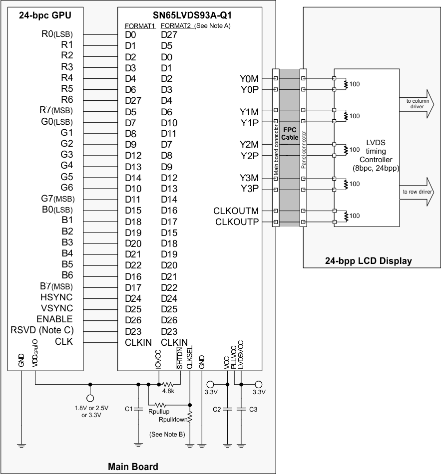
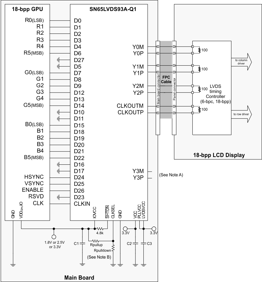
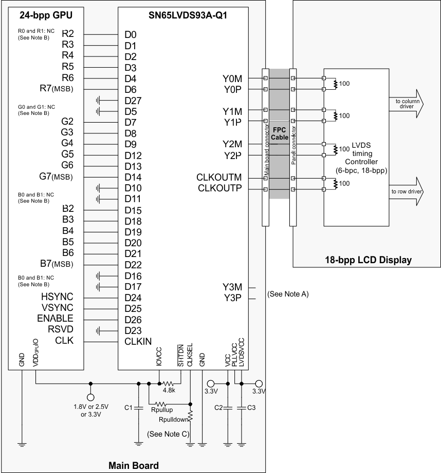
While there is no formal industry standardized specification for the input interface of LVDS LCD panels, the industry has aligned over the years on a certain data format (bit order). Figure 15 through Figure 18 show how each signal should be connected from the graphic source through the SN65LVDS93A-Q1 input, output and LVDS LCD panel input. Detailed notes are provided with each figure.

Note A. FORMAT: The majority of 24-bit LCD display panels require the two most significant bits (2 MSB ) of each color to be transferred over the 4th serial data output Y3. A few 24-bit LCD display panels require the two LSBs of each color to be transmitted over the Y3 output. The system designer needs to verify which format is expected by checking the LCD display data sheet.
- Format 1: use with displays expecting the 2 MSB to be transmitted over the 4th data channel Y3. This is the dominate data format for LCD panels.
- Format 2: use with displays expecting the 2 LSB to be transmitted over the 4th data channel.
Note B. Rpullup: install only to use rising edge triggered clocking.
Rpulldown: install only to use falling edge triggered clocking.
Rpulldown: install only to use falling edge triggered clocking.
- C1: decoupling cap for the VDDIO supply; install at least 1x0.01µF.
- C2: decoupling cap for the VDD supply; install at least 1x0.1µF and 1x0.01µF.
- C3: decoupling cap for the VDDPLL and VDDLVDS supply; install at least 1x0.1µF and 1x0.01µF.
Note C. If RSVD is not driven to a valid logic level, then an external connection to GND is recommended.
Note D. RSVD must be driven to a valid logic level. All unused SN65LVDS93A-Q1 inputs must be tied to a valid logic level.
Figure 15. 24-Bit Color Host to 24-Bit LCD Panel Application

Note A. Leave output Y3 NC.
Note B.Rpullup: install only to use rising edge triggered clocking.
Rpulldown: install only to use falling edge triggered clocking.
Figure 16. 18-Bit Color Host to 18-Bit Color LCD Panel Display Application
Rpulldown: install only to use falling edge triggered clocking.
- C1: decoupling cap for the VDDIO supply; install at least 1x0.01µF.
- C2: decoupling cap for the VDD supply; install at least 1x0.1µF and 1x0.01µF.
- C3: decoupling cap for the VDDPLL and VDDLVDS supply; install at least 1x0.1µF and 1x0.01µF.

Note A. Leave output Y3 N.C.
Note B. R3, G3, B3: this MSB of each color also connects to the 5th bit of each color for increased dynamic range of the entire color space at the expense of none-linear step sizes between each step. For linear steps with less dynamic range, connect D1, D8, and D18 to GND.
R2, G2, B2: these outputs also connects to the LSB of each color for increased, dynamic range of the entire color space at the expense of none-linear step sizes between each step. For linear steps with less dynamic range, connect D0, D7, and D15 to VCC.
R2, G2, B2: these outputs also connects to the LSB of each color for increased, dynamic range of the entire color space at the expense of none-linear step sizes between each step. For linear steps with less dynamic range, connect D0, D7, and D15 to VCC.
Note C.Rpullup: install only to use rising edge triggered clocking.
Rpulldown: install only to use falling edge triggered clocking.
Figure 17. 12-Bit Color Host to 18-Bit Color LCD Panel Display Application
Rpulldown: install only to use falling edge triggered clocking.
- C1: decoupling cap for the VDDIO supply; install at least 1x0.01µF.
- C2: decoupling cap for the VDD supply; install at least 1x0.1µF and 1x0.01µF.
- C3: decoupling cap for the VDDPLL and VDDLVDS supply; install at least 1x0.1µF and 1x0.01µF.

Note A. Leave output Y3 NC.
Note B. R0, R1, G0, G1, B0, B1: For improved image quality, the GPU should dither the 24-bit output pixel down to18-bit per pixel.
NoteC.Rpullup: install only to use rising edge triggered clocking.
Rpulldown: install only to use falling edge triggered clocking.
Figure 18. 24-Bit Color Host to 18-Bit Color LCD Panel Display Application
Rpulldown: install only to use falling edge triggered clocking.
- C1: decoupling cap for the VDDIO supply; install at least 1x0.01µF.
- C2: decoupling cap for the VDD supply; install at least 1x0.1µF and 1x0.01µF.
- C3: decoupling cap for the VDDPLL and VDDLVDS supply; install at least 1x0.1µF and 1x0.01µF.