JAJSI03K June 2004 – May 2020 SN74AUP1G32
PRODUCTION DATA
- 1 特長
- 2 アプリケーション
- 3 概要
- 4 Revision History
- 5 Pin Configuration and Functions
-
6 Specifications
- 6.1 Absolute Maximum Ratings
- 6.2 Handling Ratings
- 6.3 Recommended Operating Conditions
- 6.4 Thermal Information
- 6.5 Electrical Characteristics
- 6.6 Switching Characteristics, CL = 5 pF
- 6.7 Switching Characteristics, CL = 10 pF
- 6.8 Switching Characteristics, CL = 15 pF
- 6.9 Switching Characteristics, CL = 30 pF
- 6.10 Operating Characteristics
- 6.11 Typical Characteristics
- 7 Parameter Measurement Information
- 8 Detailed Description
- 9 Application and Implementation
- 10Power Supply Recommendations
- 11Layout
- 12Device and Documentation Support
- 13Mechanical, Packaging, and Orderable Information
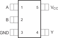
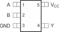
5 Pin Configuration and Functions
 Figure 5-1 DBV Package
SOT 5-pin
(Top View)
 Figure 5-3 DSF Package
SON 6-pin
(Transparent Top View)
 Figure 5-5 DCK Package
SC70 5-pin
(Top View)
See mechanical drawings at
the end of the data sheet for all package dimensions
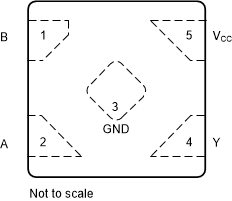
Figure 5-7 DPW Package
X2SON 5-pins
(Transparent Top View) Figure 5-2 DRL Package
SOT 5-pin
(Top View)
N.C. - No internal
connection
Figure 5-4 DRY Package
SON 6-pin
(Transparent Top View) Figure 5-6 YZP Package
DSBGA 5-balls
(Transparent Top View)
DNU - Do Not
Use
Figure 5-8 YFP Package
DSBGA 6-balls
(Transparent Top View)Pin Functions
| PIN | I/O | DESCRIPTION | |||||
|---|---|---|---|---|---|---|---|
| NAME | DRL, DCK, DBV | DPW | DRY, DSF | YZP | YFP | ||
| A | 1 | 2 | 1 | A1 | A1 | I | Input A |
| B | 2 | 1 | 2 | B1 | B1 | I | Input B |
| GND | 3 | 3 | 3 | C1 | C1 | – | Ground |
| Y | 4 | 4 | 4 | C2 | C2 | O | Output Y |
| VCC | 5 | 5 | 6 | A2 | A2 | – | Power Pin |