SCLS520E August 2003 – January 2015 SN74LV4051A-Q1
PRODUCTION DATA.
- 1 Features
- 2 Applications
- 3 Description
- 4 Revision History
- 5 Pin Configuration and Functions
- 6 Specifications
- 7 Parameter Measurement Information
- 8 Detailed Description
- 9 Application and Implementation
- 10Power Supply Recommendations
- 11Layout
- 12Device and Documentation Support
- 13Mechanical, Packaging, and Orderable Information
パッケージ・オプション
デバイスごとのパッケージ図は、PDF版データシートをご参照ください。
メカニカル・データ(パッケージ|ピン)
- PW|16
- DW|16
- D|16
サーマルパッド・メカニカル・データ
発注情報
8 Detailed Description
8.1 Overview
This device is an 8-channel analog multiplexer. A multiplexer is used when several signals must share the same device or resource. This device allows the selection of one of these signals at a time, for analysis or propagation.
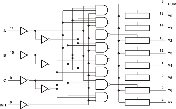
8.2 Functional Block Diagram
8.3 Feature Description
This device contains one 8-channel multiplexer for use in a variety of applications, and can also be configured as demultiplexer by using the COM pin as an input and the Yx pins as outputs. This device is qualified for automotive applications and has an extended temperature range of –40°C to 125°C (maximum depends on package type).
8.4 Device Functional Modes
Table 1. Function Table
| INPUTS | ON CHANNEL |
|||
|---|---|---|---|---|
| INH | C | B | A | |
| L | L | L | L | Y0 |
| L | L | L | H | Y1 |
| L | L | H | L | Y2 |
| L | L | H | H | Y3 |
| L | H | L | L | Y4 |
| L | H | L | H | Y5 |
| L | H | H | L | Y6 |
| L | H | H | H | Y7 |
| H | X | X | X | None |