SCLS520E August 2003 – January 2015 SN74LV4051A-Q1
PRODUCTION DATA.
- 1 Features
- 2 Applications
- 3 Description
- 4 Revision History
- 5 Pin Configuration and Functions
- 6 Specifications
- 7 Parameter Measurement Information
- 8 Detailed Description
- 9 Application and Implementation
- 10Power Supply Recommendations
- 11Layout
- 12Device and Documentation Support
- 13Mechanical, Packaging, and Orderable Information
パッケージ・オプション
デバイスごとのパッケージ図は、PDF版データシートをご参照ください。
メカニカル・データ(パッケージ|ピン)
- PW|16
- DW|16
- D|16
サーマルパッド・メカニカル・データ
発注情報
5 Pin Configuration and Functions
D, DW, or PW Package
16 Pins
Top View
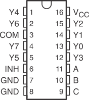
Pin Functions
| PIN | I/O | DESCRIPTION | |
|---|---|---|---|
| NAME | NO. | ||
| Y4 | 1 | I(1) | Input to mux |
| Y6 | 2 | I(1) | Input to mux |
| COM | 3 | O(1) | Output of mux |
| Y7 | 4 | I(1) | Input to mux |
| Y5 | 5 | I(1) | Input to mux |
| INH | 6 | I(1) | Enables the outputs of the device. Logic low level with turn the outputs on, high level will turn them off. |
| GND | 7 | — | Ground |
| GND | 8 | — | Ground |
| C | 9 | I | Selector line for outputs (see Device Functional Modes for specific information) |
| B | 10 | I | Selector line for outputs (see Device Functional Modes for specific information) |
| A | 11 | I | Selector line for outputs (see Device Functional Modes for specific information) |
| Y3 | 12 | I(1) | Input to mux |
| Y0 | 13 | I(1) | Input to mux |
| Y1 | 14 | I(1) | Input to mux |
| Y2 | 15 | I(1) | Input to mux |
| Vcc | 16 | I | Device power input |
(1) These I/O descriptions represent the device when used as a multiplexer, when this device is operated as a demultiplexer pins Y0-Y7 may be considered outputs (O) and the COM pin may be considered inputs (I).
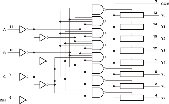 Figure 1. Logic Diagram (Positive Logic)