JAJSD24 March 2017 SN74LVC1G86-Q1
PRODUCTION DATA.
9 Application and Implementation
NOTE
Information in the following applications sections is not part of the TI component specification, and TI does not warrant its accuracy or completeness. TI’s customers are responsible for determining suitability of components for their purposes. Customers should validate and test their design implementation to confirm system functionality.
9.1 Application Information
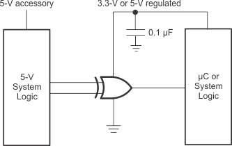
The SN74LVC1G86-Q1 device can accept input voltages up to 5.5 V at any valid VCC which makes the device suitable for down translation. This feature of the SN74LVC1G86-Q1 makes it ideal for various bus interface applications.
9.2 Typical Application
 Figure 4. Typical Application Schematic
9.2.1 Design Requirements
This device uses CMOS technology and has balanced output drive. Take care to avoid bus contention because it can drive currents that would exceed maximum limits. The high drive will also create fast edges into light loads, so routing and load conditions should be considered to prevent ringing.
9.2.2 Detailed Design Procedure
- Recommended Input Conditions
- For rise time and fall time specifications, see Δt/ΔV in the Recommended Operating Conditions table.
- For specified High and low levels, see VIH and VIL in the Recommended Operating Conditions table.
- Inputs are overvoltage tolerant allowing them to go as high as 5.5 V at any valid VCC.
- Recommended Output Conditions
- Load currents should not exceed 32 mA per output and 50 mA total for the part.
- Outputs should not be pulled above VCC.
9.2.3 Application Curve
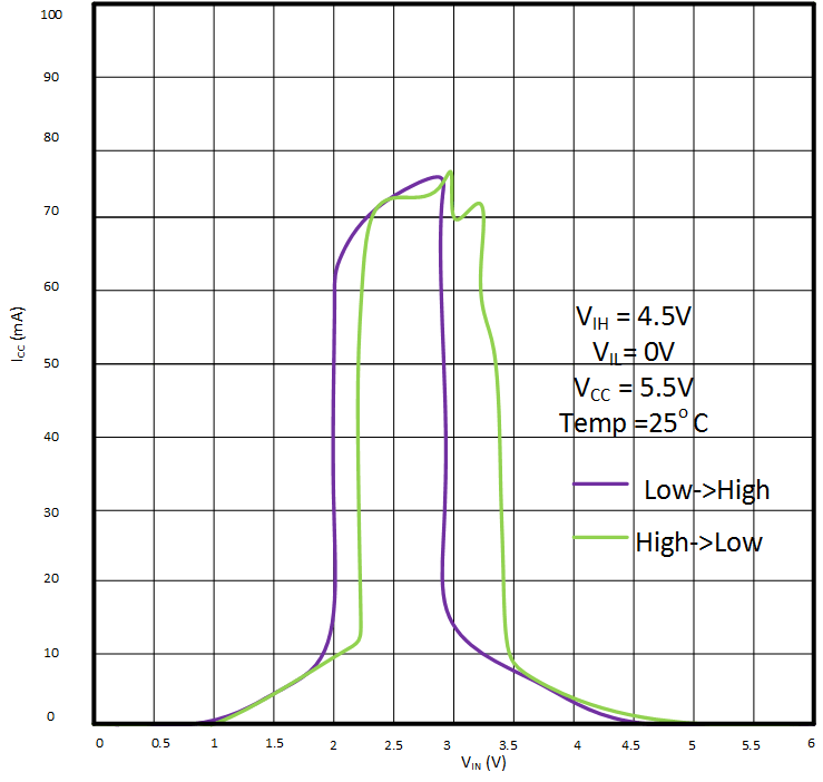
 Figure 5. ICC vs. VIN