JAJSD24 March   2017 SN74LVC1G86-Q1

PRODUCTION DATA.  

  1. 特長
  2. アプリケーション
  3. 概要
  4. 改訂履歴
  5. Pin Configuration and Functions
  6. Specifications
    1. 6.1 Absolute Maximum Ratings
    2. 6.2 ESD Ratings
    3. 6.3 Recommended Operating Conditions
    4. 6.4 Thermal Information
    5. 6.5 Electrical Characteristics
    6. 6.6 Switching Characteristics, CL = 30 pF or 50 pF
    7. 6.7 Operating Characteristics
    8. 6.8 Typical Characteristics
  7. Parameter Measurement Information
  8. Detailed Description
    1. 8.1 Overview
    2. 8.2 Functional Block Diagram
    3. 8.3 Feature Description
      1. 8.3.1 Balanced High-Drive CMOS Push-Pull Outputs
      2. 8.3.2 Standard CMOS Inputs
      3. 8.3.3 Clamp Diodes
      4. 8.3.4 Partial Power Down (Ioff)
      5. 8.3.5 Over-voltage Tolerant Inputs
    4. 8.4 Function Table
  9. Application and Implementation
    1. 9.1 Application Information
    2. 9.2 Typical Application
      1. 9.2.1 Design Requirements
      2. 9.2.2 Detailed Design Procedure
      3. 9.2.3 Application Curve
  10. 10Power Supply Recommendations
  11. 11Layout
    1. 11.1 Layout Guidelines
    2. 11.2 Layout Example
  12. 12デバイスおよびドキュメントのサポート
    1. 12.1 ドキュメントの更新通知を受け取る方法
    2. 12.2 コミュニティ・リソース
    3. 12.3 商標
    4. 12.4 静電気放電に関する注意事項
    5. 12.5 Glossary
  13. 13メカニカル、パッケージ、および注文情報

パッケージ・オプション

メカニカル・データ(パッケージ|ピン)
サーマルパッド・メカニカル・データ
発注情報

Layout

Layout Guidelines

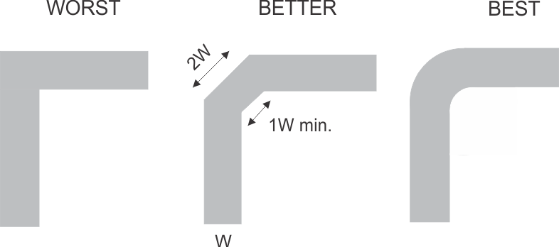
Even low data rate digital signals can have high frequency signal components due to fast edge rates. When a PCB trace turns a corner at a 90° angle, a reflection can occur. A reflection occurs primarily because of the change of width of the trace. At the apex of the turn, the trace width increases to 1.414 times the width. This increase upsets the transmission-line characteristics, especially the distributed capacitance and self–inductance of the trace which results in the reflection. Not all PCB traces can be straight and therefore some traces must turn corners. Figure 6 shows progressively better techniques of rounding corners. Only the last example (BEST) maintains constant trace width and minimizes reflections.

Layout Example

SN74LVC1G86-Q1 layout_scds357.gif Figure 6. Trace Example