SCES427B February 2003 – June 2014 SN74LVCR16245A
PRODUCTION DATA.
- 1 Features
- 2 Applications
- 3 Description
- 4 Simplified Schematic
- 5 Revision History
- 6 Pin Configuration and Functions
- 7 Specifications
- 8 Parameter Measurement Information
- 9 Detailed Description
- 10Application and Implementation
- 11Power Supply Recommendations
- 12Layout
- 13Device and Documentation Support
- 14Mechanical, Packaging, and Orderable Information
パッケージ・オプション
デバイスごとのパッケージ図は、PDF版データシートをご参照ください。
メカニカル・データ(パッケージ|ピン)
- DGG|48
- DL|48
- DGV|48
サーマルパッド・メカニカル・データ
発注情報
9 Detailed Description
9.1 Overview
The SN74LVCR16245A device is designed for asynchronous communication between data buses. The logic levels of the direction-control (DIR) input and the output-enable (OE) input activate either the B-port outputs or the A-port outputs or place both output ports into the high-impedance mode. The device transmits data from the A bus to the B bus when the B-port outputs are activated, and from the B bus to the A bus when the A-port outputs are activated. The input circuitry on both A and B ports always is active and must have a logic HIGH or LOW level applied to prevent excess ICC and ICCZ.
All inputs and outputs have equivalent 26-Ω resistors that will slow the edges of the output and reduce switching noise caused by long capacitive etch runs or cables.
To ensure the high-impedance state during power up or power down, OE should be tied to VCC through a pullup resistor. The minimum value of the resistor is determined by the current-sinking capability of the driver. Inputs can be driven from either 3.3-V or 5-V devices. This feature allows the use of these devices as translators in a mixed 3.3-V/5-V system environment.
This device is fully specified for partial-power-down applications using Ioff. The Ioff circuitry disables the outputs, preventing damaging current backflow through the device when it is powered down.
9.2 Functional Block Diagram
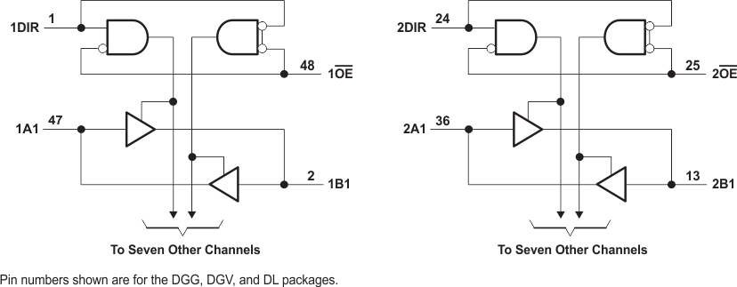 Figure 4. Logic Diagram (Positive Logic)
9.3 Feature Description
- Wide operating voltage range
- Operates from 1.65 V to 3.6 V
- Allows down voltage translation
- Inputs accept voltages to 5.5 V
- Ioff feature
- Allows voltages on the inputs and outputs when VCC is 0 V
9.4 Device Functional Modes
Table 1. Function Table
(Each 8-Bit Section)
| INPUTS | OPERATION | |
|---|---|---|
| OE | DIR | |
| L | L | B data to A bus |
| L | H | A data to B bus |
| H | X | Isolation |