SLOS739A July 2012 – March 2016 TAS5721
PRODUCTION DATA.
- 1 Features
- 2 Applications
- 3 Description
- 4 Revision History
- 5 Device Comparison Table
- 6 Pin Configuration and Functions
-
7 Specifications
- 7.1 Absolute Maximum Ratings
- 7.2 ESD Ratings
- 7.3 Recommended Operating Conditions
- 7.4 Thermal Information
- 7.5 Electrical Characteristics - I/O Pin Characteristics
- 7.6 Master Clock Characteristics
- 7.7 Speaker Amplifier Characteristics
- 7.8 Headphone Amplifier and Line Driver Characteristics
- 7.9 Protection Characteristics
- 7.10 I2C Serial Control Port Requirements and Specifications
- 7.11 Serial Audio Port Timing
- 7.12 Typical Characteristics
- 8 Parameter Measurement Information
-
9 Detailed Description
- 9.1 Overview
- 9.2 Functional Block Diagram
- 9.3
Feature Description
- 9.3.1 Power Supply
- 9.3.2 I2C Address Selection and Fault Output
- 9.3.3 Device Protection System
- 9.3.4 Clock, Auto Detection, and PLL
- 9.3.5 PWM Section
- 9.3.6 SSTIMER Functionality
- 9.3.7 2.1-Mode Support
- 9.3.8 PBTL-Mode Support
- 9.3.9 I2C Serial Control Interface
- 9.3.10 Dynamic Range Control (DRC)
- 9.3.11 Bank Switching
- 9.3.12 Serial Data Interface
- 9.3.13 DirectPath Headphone/Line Driver
- 9.4 Device Functional Modes
- 9.5 Programming
- 9.6
Register Maps
- 9.6.1 Clock Control Register (0x00)
- 9.6.2 Device ID Register (0x01)
- 9.6.3 Error Status Register (0x02)
- 9.6.4 System Control Register 1 (0x03)
- 9.6.5 Serial Data Interface Register (0x04)
- 9.6.6 System Control Register 2 (0x05)
- 9.6.7 Soft Mute Register (0x06)
- 9.6.8 Volume Registers (0x07, 0x08, 0x09, 0x0A)
- 9.6.9 Volume Configuration Register (0x0E)
- 9.6.10 Modulation Limit Register (0x10)
- 9.6.11 Interchannel Delay Registers (0x11, 0x12, 0x13, and 0x14)
- 9.6.12 Pwm Shutdown Group Register (0x19)
- 9.6.13 Start/stop Period Register (0x1A)
- 9.6.14 Oscillator Trim Register (0x1B)
- 9.6.15 BKND_ERR Register (0x1C)
- 9.6.16 Input Multiplexer Register (0x20)
- 9.6.17 Channel 4 Source Select Register (0x21)
- 9.6.18 PWM Output MUX Register (0x25)
- 9.6.19 DRC Control (0x46)
- 9.6.20 Bank Switch and EQ Control (0x50)
-
10Application and Implementation
- 10.1 Application Information
- 10.2 Typical Application
- 10.3 System Examples
- 11Power Supply Recommendations
- 12Layout
- 13Device and Documentation Support
- 14Mechanical, Packaging, and Orderable Information
パッケージ・オプション
メカニカル・データ(パッケージ|ピン)
- DCA|48
サーマルパッド・メカニカル・データ
- DCA|48
発注情報
7 Specifications
7.1 Absolute Maximum Ratings
over operating free-air temperature range (unless otherwise noted). (1)| MIN | MAX | UNIT | ||
|---|---|---|---|---|
| Supply voltage | DVDD, AVDD, DRVDD | –0.3 | 3.6 | V |
| PVDD | –0.3 | 30 | V | |
| DR_INx | –0.3 | DRVDD + 6 | V | |
| Input voltage | 3.3-V digital input | –0.5 | DVDD + 0.5 | V |
| 5-V tolerant(2) digital input (except MCLK) | –0.5 | DVDD + 2.5(4) | ||
| 5-V tolerant MCLK input | –0.5 | AVDD + 2.5(4) | ||
| SPK_OUTx to GND | 32(3) | V | ||
| BSTRPx to GND | 39(3) | V | ||
| Operating free-air temperature | 0 | 85 | °C | |
| Storage temperature, Tstg | –40 | 125 | °C | |
(1) Stresses beyond those listed under Absolute Maximum Ratings may cause permanent damage to the device. These are stress ratings only and functional operation of the device at these or any other conditions beyond those indicated under Recommended Operating Conditions is not implied. Exposure to absolute-maximum conditions for extended periods may affect device reliability.
(2) 5-V tolerant inputs are PDN, RST, SCLK, LRCLK, MCLK, SDIN, SDA, and SCL.
(3) DC voltage + peak AC waveform measured at the pin should be below the allowed limit for all conditions.
(4) Maximum pin voltage should not exceed 6 V.
7.2 ESD Ratings
| VALUE | UNIT | |||
|---|---|---|---|---|
| V(ESD) | Electrostatic discharge | Human-body model (HBM), per ANSI/ESDA/JEDEC JS-001(1) | ±1000 | V |
| Charged-device model (CDM), per JEDEC specification JESD22-C101(2) | ±250 | |||
(1) JEDEC document JEP155 states that 500-V HBM allows safe manufacturing with a standard ESD control process.
(2) JEDEC document JEP157 states that 250-V CDM allows safe manufacturing with a standard ESD control process.
7.3 Recommended Operating Conditions
| MIN | NOM | MAX | UNIT | |||
|---|---|---|---|---|---|---|
| xVDD | Digital, analog, headphone supply voltage | 3 | 3.3 | 3.6 | V | |
| PVDD | Half-bridge supply voltage | 8 | 26.4(1) | V | ||
| VIH | High-level input voltage | 5-V tolerant | 2 | V | ||
| VIL | Low-level input voltage | 5-V tolerant | 0.8 | V | ||
| TA | Operating ambient temperature | 0 | 85 | °C | ||
| TJ (2) | Operating junction temperature | 0 | 125 | °C | ||
| RSPK
(SE, BTL, and PBTL) |
Minimum supported speaker impedance | Output filter: L = 15 μH, C = 330 nF | 4 | 8 | Ω | |
| Lo(BTL) | Output-filter inductance | Minimum output inductance under short-circuit condition |
10 | μH | ||
| RHP | Headphone mode load impedance | 16 | 32 | Ω | ||
| RLD | Line-diver mode load impedance | 0.6 | 10 | kΩ | ||
(1) For operation at PVDD levels greater than 18 V, the modulation limit must be set to 93.8% via the control port register 0x10.
(2) Continuous operation above the recommended junction temperature may result in reduced reliability and/or lifetime of the device.
7.4 Thermal Information
| THERMAL METRIC(1) | TAS5721 | UNIT | |
|---|---|---|---|
| DCA (HTSSOP) | |||
| 48 PINS | |||
| RθJA | Junction-to-ambient thermal resistance | 27.9 | °C/W |
| RθJC(top) | Junction-to-case (top) thermal resistance | 20.7 | °C/W |
| RθJB | Junction-to-board thermal resistance | 13 | °C/W |
| ψJT | Junction-to-top characterization parameter | 0.3 | °C/W |
| ψJB | Junction-to-board characterization parameter | 6.7 | °C/W |
| RθJC(bot) | Junction-to-case (bottom) thermal resistance | 1.1 | °C/W |
(1) For more information about traditional and new thermal metrics, see the Semiconductor and IC Package Thermal Metrics application report, SPRA953.
7.5 Electrical Characteristics – I/O Pin Characteristics
PVDD = 18 V, AVDD = DRVDD = DVDD = 3.3 V, external components per Typical Application diagrams, and in accordance with recommended operating conditions (unless otherwise specified).| PARAMETER | TEST CONDITIONS | MIN | TYP | MAX | UNIT | ||
|---|---|---|---|---|---|---|---|
| VOH | High-level output voltage | ADR/FAULT and SDA | IOH = –4 mA DVDD = AVDD = 3 V |
2.4 | V | ||
| VOL | Low-level output voltage | IOL = 4 mA DVDD = AVDD = 3 V |
0.5 | ||||
| IIL | Low-level input current | Digital Inputs | VI < VIL ; DVDD = AVDD = 3.6 V |
75 | μA | ||
| IIH | High-level input current | VI > VIH ; DVDD = AVDD = 3.6 V |
75 | ||||
| IDD | 3.3 V supply current | 3.3 V supply voltage (DVDD, AVDD) | Normal mode | 48 | 70 | mA | |
| Reset (RST = low, PDN = high, DR_SD = low) | 21 | 38 | |||||
| tw(RST) | Pulse duration, RST active | RST | 100 | μs | |||
| td(I2C_ready) | Time before the I2C port is able communicate after RST goes high | 12 | ms | ||||
7.6 Master Clock Characteristics(1)
PVDD = 18 V, AVDD = DRVDD = DVDD = 3.3 V, external components per Typical Application diagrams, and in accordance with recommended operating conditions (unless otherwise specified).| PARAMETER | TEST CONDITIONS | MIN | TYP | MAX | UNIT | |
|---|---|---|---|---|---|---|
| fMCLK | MCLK frequency | 2.8224 | 24.576 | MHz | ||
| MCLK duty cycle | 40% | 50% | 60% | |||
| tr(MCLK) / tf(MCLK) | Rise/fall time for MCLK | 5 | ns | |||
(1) For clocks related to the serial audio port, please see Serial Audio Port Timing
7.7 Speaker Amplifier Characteristics
TA = 25°C, PVDD = 18 V, AVDD = DRVDD = DVDD = 3.3 V, audio input signal =1 kHz sine wave, BTL, AD mode, fS = 48 kHz, RSPK = 8 Ω, AES17 filter, fPWM = 384 kHz, external components per Typical Application diagrams, and in accordance with recommended operating conditions (unless otherwise specified).| PARAMETER | TEST CONDITIONS | MIN | TYP | MAX | UNIT | ||
|---|---|---|---|---|---|---|---|
| PoSPK (BTL) | Power output per channel of speaker amplifier when used in BTL mode (2) | PVDD = 18 V, RSPK = 8Ω, 1-kHz input signal | 10 | W | |||
| PVDD = 12 V, RSPK = 8Ω, 10% THD+N, 1-kHz input signal | 8.8 | ||||||
| PVDD = 12 V, RSPK = 8Ω, 7% THD+N, 1-kHz input signal | 8.3 | ||||||
| PVDD = 8 V, RSPK = 8Ω, 10% THD+N, 1-kHz input signal | 4 | ||||||
| PVDD = 8 V, RSPK = 8Ω, 7% THD+N, 1-kHz input signal | 3.8 | ||||||
| PoSPK (PBTL) | Power output per channel of speaker amplifier when used in PBTL mode (2) | PVDD = 12 V, RSPK = 4Ω, 10% THD+N, 1-kHz input signal |
10 | W | |||
| PVDD = 12 V, RSPK = 4Ω, 7% THD+N, 1-kHz input signal |
10 | ||||||
| PVDD = 18 V, RSPK = 4Ω, 1-kHz input signal |
10 | ||||||
| PoSPK (SE) | Power output per channel of speaker amplifier when used in SE mode (2) | PVDD = 12 V, RSPK = 4 Ω, 10% THD+N, 1-kHz input signal |
4.3 | W | |||
| PVDD = 24 V, RSPK = 4 Ω, 10% THD+N, 1-kHz input signal |
5.5 | ||||||
| THD+N | Total harmonic distortion + noise | PVDD = 18 V, PO = 1 W | 0.07% | ||||
| PVDD = 12 V, PO = 1 W | 0.11% | ||||||
| PVDD = 8 V, PO = 1 W | 0.2% | ||||||
| ICN | Idle channel noise | A-weighted | 61 | μV | |||
| Crosstalk | PO = 1 W, f = 1 kHz (BD Mode), PVDD = 24 V | 58 | dB | ||||
| PO =1 W, f = 1 kHz (AD Mode), PVDD = 24 V | 48 | dB | |||||
| SNR | Signal-to-noise ratio(1) | A-weighted, f = 1 kHz, maximum power at THD < 1% | 106 | dB | |||
| fPWM | Output switching frequency | 11.025/22.05/44.1-kHz data rate ±2% | 352.8 | kHz | |||
| 48/24/12/8/16/32-kHz data rate ±2% | 384 | ||||||
| IPVDD | Supply current | No load (PVDD) | Normal mode | 32 | 50 | mA | |
| Reset (RST = low, PDN = high) | 5 | 8 | |||||
| rDS(on) | Drain-to-source resistance (for each of the Low-Side and High-Side Devices) | TJ = 25°C, includes metallization resistance | 200 | mΩ | |||
| RPD | Internal pulldown resistor at the output of each half-bridge | Connected when drivers are in the high-impedance state to provide bootstrap capacitor charge. | 3 | kΩ | |||
(1) SNR is calculated relative to 0-dBFS input level.
(2) Power levels are thermally limited.
7.8 Headphone Amplifier and Line Driver Characteristics
TA = 25°C, PVDD = 18 V, AVDD = DRVDD = DVDD = 3.3 V, audio input signal =1 kHz sine wave, BTL, AD mode, fS = 48 kHz, RSPK = 8 Ω, AES17 filter, fPWM = 384 kHz, external components per Typical Application diagrams, and in accordance with recommended operating conditions (unless otherwise specified).| PARAMETER | TEST CONDITIONS | MIN | TYP | MAX | UNIT | |
|---|---|---|---|---|---|---|
| PoHP | Power output per channel of headphone amplifier | DRVDD = 3.3 V (RHP = 32; THD = 1%) | 50 | mW | ||
| AVDR | Gain for headphone amplifier and line driver | Adjustable through Rin and Rfb | - | dB | ||
| SNRHP | Signal-to-noise ratio (headphone mode) | Rhp = 32 | 101 | dB | ||
| SNRLD | Signal-to-noise ratio (line driver mode) | 2-VRMS output | 105 | dB | ||
7.9 Protection Characteristics
TA = 25°C, PVDD = 18 V, AVDD = DRVDD = DVDD = 3.3 V, audio input signal =1 kHz sine wave, BTL, AD mode, fS = 48 kHz, RSPK = 8 Ω, AES17 filter, fPWM = 384 kHz, external components per Typical Application diagrams, and in accordance with recommended operating conditions (unless otherwise specified).| MIN | TYP | MAX | UNIT | ||||
|---|---|---|---|---|---|---|---|
| Vuvp(fall) | Undervoltage protection limit | PVDD falling | 4 | V | |||
| Vuvp(rise) | Undervoltage protection limit | PVDD rising | 4.1 | V | |||
| OTE | Overtemperature error threshold | 150 | °C | ||||
| ΔOTE | Variation in overtemperature detection circuit | ±15 | °C | ||||
| IOCE | Overcurrent limit protection threshold | 3 | A | ||||
| tOCE | Overcurrent response time | 150 | ns | ||||
7.10 I2C Serial Control Port Requirements and Specifications
PVDD = 18 V, AVDD = DRVDD = DVDD = 3.3 V, external components per Typical Application diagrams, and in accordance with recommended operating conditions (unless otherwise specified).| MIN | MAX | UNIT | |||
|---|---|---|---|---|---|
| fSCL | Frequency, SCL | No wait states | 400 | kHz | |
| tw(H) | Pulse duration, SCL high | 0.6 | μs | ||
| tw(L) | Pulse duration, SCL low | 1.3 | μs | ||
| tr | Rise time, SCL and SDA | 300 | ns | ||
| tf | Fall time, SCL and SDA | 300 | ns | ||
| tsu1 | Setup time, SDA to SCL | 100 | ns | ||
| th1 | Hold time, SCL to SDA | 0 | ns | ||
| t(buf) | Bus free time between stop and start conditions | 1.3 | μs | ||
| tsu2 | Setup time, SCL to start condition | 0.6 | μs | ||
| th2 | Hold time, start condition to SCL | 0.6 | μs | ||
| tsu3 | Setup time, SCL to stop condition | 0.6 | μs | ||
| CL | Load capacitance for each bus line | 400 | pF | ||
7.11 Serial Audio Port Timing
PVDD = 18 V, AVDD = DRVDD = DVDD = 3.3 V, audio input signal =1 kHz sine wave, BTL, AD mode, fS = 48 kHz, RSPK = 8 Ω, AES17 filter, fPWM = 384 kHz, external components per Typical Application diagrams, and in accordance with recommended operating conditions (unless otherwise specified).| MIN | TYP | MAX | UNIT | |||
|---|---|---|---|---|---|---|
| fSCLKIN | Frequency, SCLK 32 × fS, 48 × fS, 64 × fS | CL = 30 pF | 1.024 | 12.288 | MHz | |
| tsu1 | Setup time, LRCLK to SCLK rising edge | 10 | ns | |||
| th1 | Hold time, LRCLK from SCLK rising edge | 10 | ns | |||
| tsu2 | Setup time, SDIN to SCLK rising edge | 10 | ns | |||
| th2 | Hold time, SDIN from SCLK rising edge | 10 | ns | |||
| LRCLK frequency | 8 | 48 | 48 | kHz | ||
| SCLK duty cycle | 40% | 50% | 60% | |||
| LRCLK duty cycle | 40% | 50% | 60% | |||
| SCLK rising edges between LRCLK rising edges | 32 | 64 | SCLK edges | |||
| t(edge) | LRCLK clock edge with respect to the falling edge of SCLK | –1/4 | 1/4 | SCLK period | ||
| tr/tf | Rise/fall time for SCLK/LRCLK | 8 | ns | |||
| LRCLK allowable drift before LRCLK reset | 4 | MCLK Periods | ||||
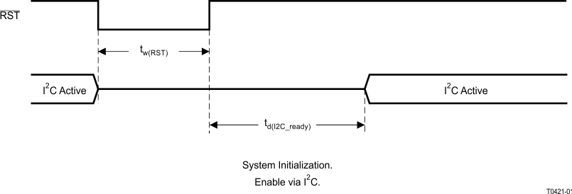
NOTE:
On power up, it is recommended that the TAS5721 RST be held LOW for at least 100 μs after DVDD has reached 3 V.NOTE:
If RST is asserted LOW while PDN is LOW, then RST must continue to be held LOW for at least 100 μs after PDN is deasserted (HIGH). Figure 2. SCL and SDA Timing
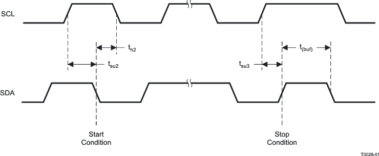 Figure 3. Start and Stop Conditions Timing
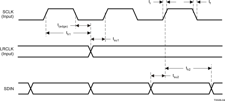 Figure 4. Serial Audio Port Timing
7.12 Typical Characteristics
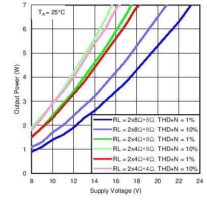 Figure 5. Output Power vs PVDD IN 2.1 Mode
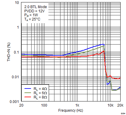 Figure 7. Total Harmonic Distortion + Noise vs Frequency in 2.0 Mode With PVDD = 12 V
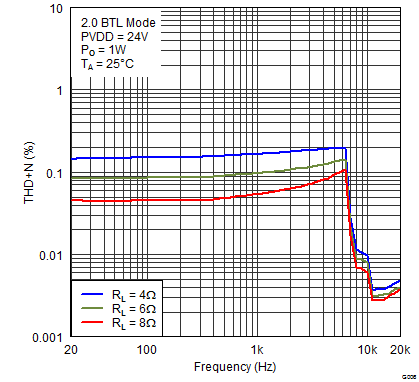 Figure 9. Total Harmonic Distortion + Noise vs Frequency in 2.0 Mode With PVDD = 24 V
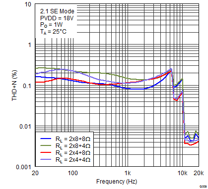 Figure 11. Total Harmonic Distortion + Noise vs Frequency in 2.1 Mode With PVDD = 18 V
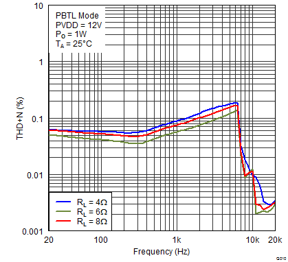 Figure 13. Total Harmonic Distortion + Noise vs Frequency in PBTL Mode With PVDD = 12 V
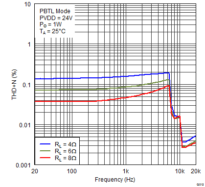 Figure 15. Total Harmonic Distortion + Noise vs Frequency in PBTL Mode With PVDD = 24 V
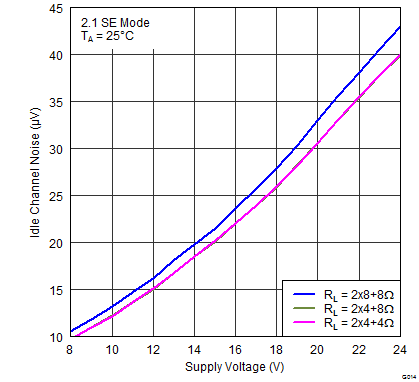 Figure 17. 2.1 Idle Channel Noise vs PVDD
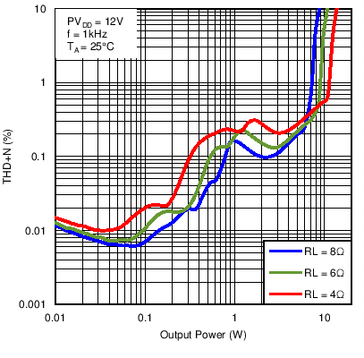 Figure 19. Total Harmonic Distortion + Noise vs Output Power in 2.0 Mode With PVDD = 12 V
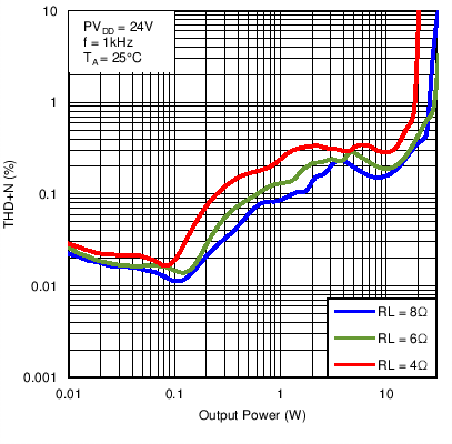 Figure 21. Total Harmonic Distortion + Noise vs Output Power in 2.0 Mode With PVDD = 24 V
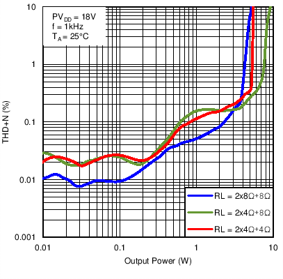 Figure 23. Total Harmonic Distortion + Noise vs Output Power in 2.1 Mode With PVDD = 18 V
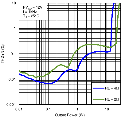 Figure 25. Total Harmonic Distortion + Noise vs Output Power in PBTL Mode With PVDD = 12 V
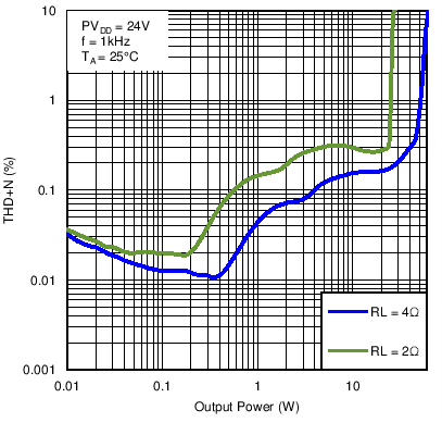 Figure 27. Total Harmonic Distortion + Noise vs Output Power in PBTL Mode With PVDD = 24 V
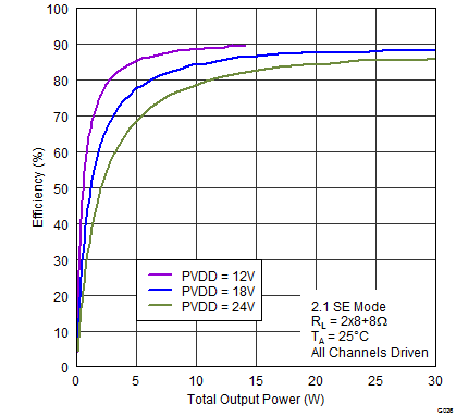
All channels driven
Figure 29. Efficiency vs Output Power in 2.1 Mode
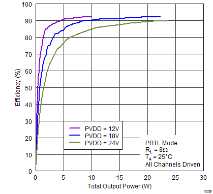
All channels driven
Figure 31. Efficiency vs Output Power in PBTL Mode
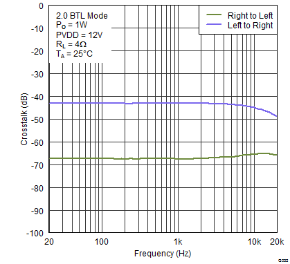 Figure 33. Crosstalk vs Frequency in 2.0 Mode
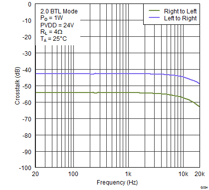 Figure 35. Crosstalk vs Frequency in 2.0 Mode
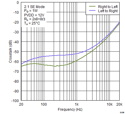 Figure 37. Crosstalk vs Frequency in 2.1 Mode
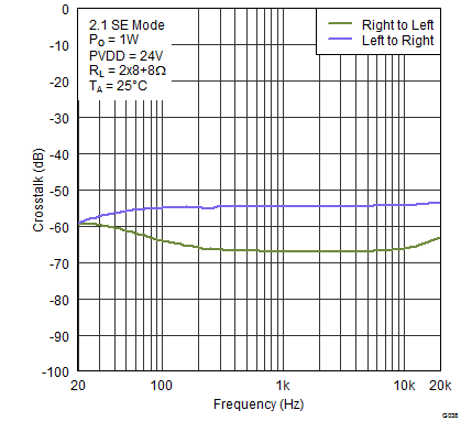 Figure 39. Crosstalk vs Frequency in 2.1 Mode
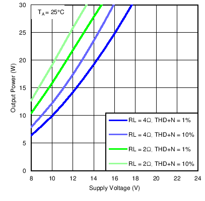 Figure 6. Output Power vs PVDD in PBTL Mode
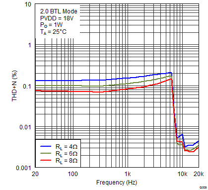 Figure 8. Total Harmonic Distortion + Noise vs Frequency in 2.0 Mode With PVDD = 18 V
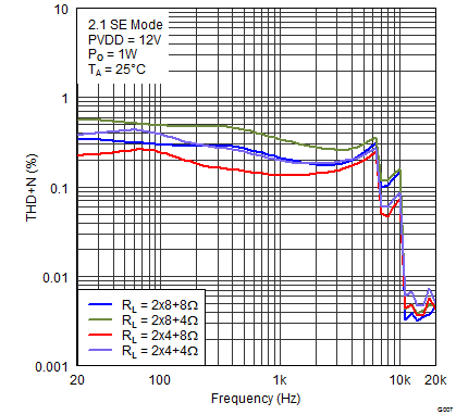 Figure 10. Total Harmonic Distortion + Noise vs Frequency in 2.1 Mode With PVDD = 12 V
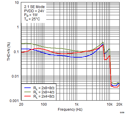 Figure 12. Total Harmonic Distortion + Noise vs Frequency in 2.1 Mode With PVDD = 24 V
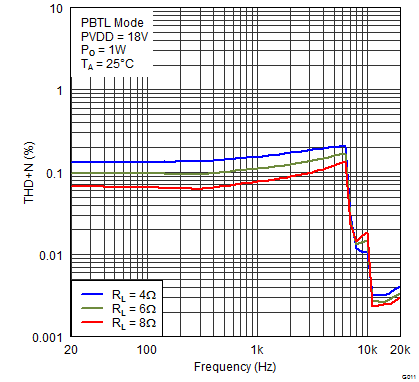 Figure 14. Total Harmonic Distortion + Noise vs Frequency in PBTL Mode With PVDD = 18 V
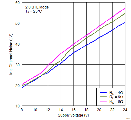 Figure 16. 2.0 Idle Channel Noise vs PVDD
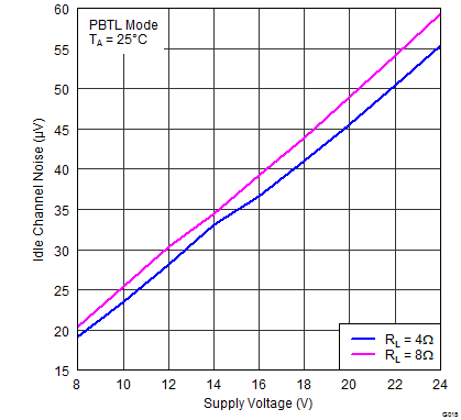 Figure 18. PBTL Idle Channel Noise vs PVDD
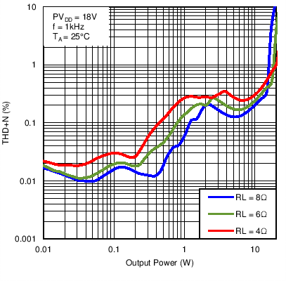 Figure 20. Total Harmonic Distortion + Noise vs Output Power in 2.0 Mode With PVDD = 18 V
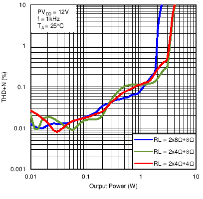 Figure 22. Total Harmonic Distortion + Noise vs Output Power in 2.1 Mode With PVDD = 12 V
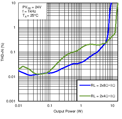 Figure 24. Total Harmonic Distortion + Noise vs Output Power in 2.1 Mode With PVDD = 24 V
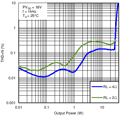 Figure 26. Total Harmonic Distortion + Noise vs Output Power in PBTL Mode With PVDD = 18 V
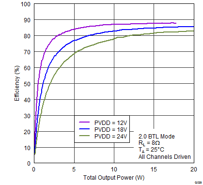
All channels driven
Figure 28. Efficiency vs Output Power in 2.0 Mode
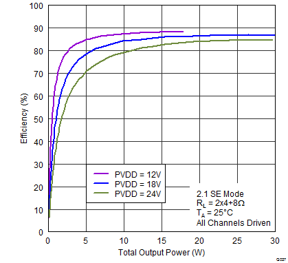
All channels driven
Figure 30. Efficiency vs Output Power in 2.1 Mode
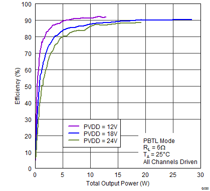
All channels driven
Figure 32. Efficiency vs Output Power in PBTL Mode
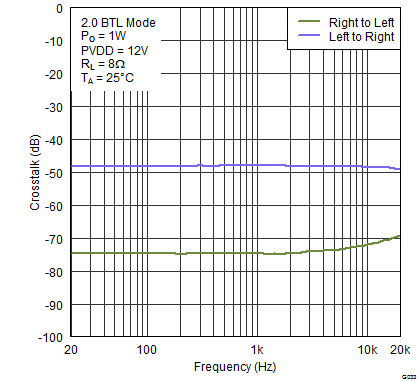 Figure 34. Crosstalk vs Frequency in 2.0 Mode
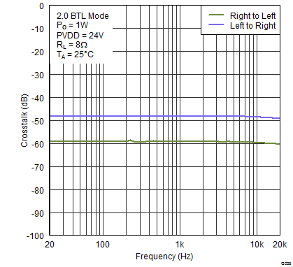 Figure 36. Crosstalk vs Frequency in 2.0 Mode
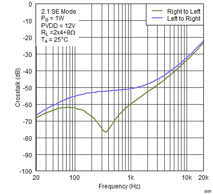 Figure 38. Crosstalk vs Frequency in 2.1 Mode
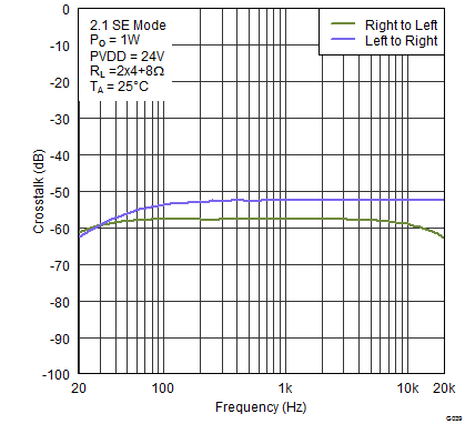 Figure 40. Crosstalk vs Frequency in 2.1 Mode
7.12.1 Headphone Typical Characteristics
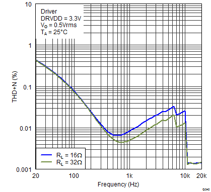 Figure 41. Total Harmonic Distortion + Noise vs Frequency Headphone With DRVDD = 3.3 V
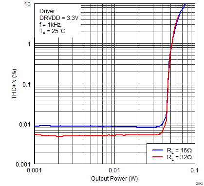 Figure 43. Total Harmonic Distortion + Noise vs Output Power Headphone With DRVDD = 3.3 V
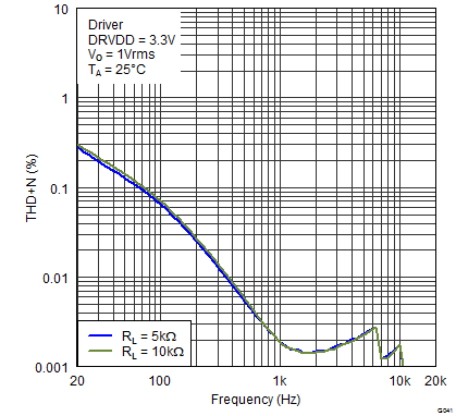 Figure 42. Total Harmonic Distortion + Noise vs Frequency Headphone With DRVDD = 3.3 V
7.12.2 Line Driver Typical Characteristics
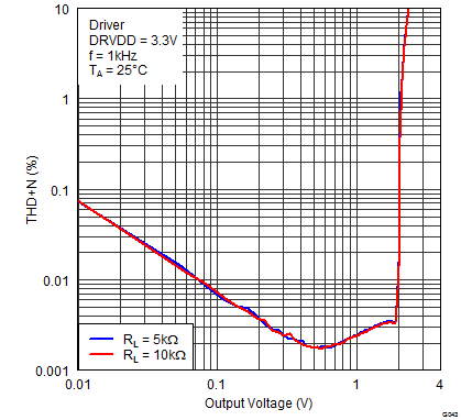 Figure 44. Total Harmonic Distortion + Noise vs Output Voltage Headphone With DRVDD = 3.3 V
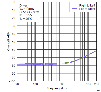 Figure 46. Crosstalk vs Frequency Headphone With DRVDD = 3.3 V
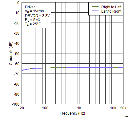 Figure 45. Crosstalk vs Frequency Headphone With DRVDD = 3.3 V
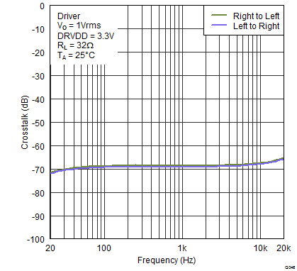 Figure 47. Crosstalk vs Frequency Headphone With DRVDD = 3.3 V