JAJST56D October 2001 – February 2024 TFP410
PRODUCTION DATA
- 1
- 1 特長
- 2 アプリケーション
- 3 概要
- 4 Pin Configuration and Functions
- 5 Specifications
-
6 Detailed Description
- 6.1 Overview
- 6.2 Functional Block Diagram
- 6.3 Feature Description
- 6.4 Device Functional Modes
- 6.5 Programming
- 6.6
Register Maps
- 6.6.1 VEN_ID Register (Sub-Address = 01−00 ) [reset = 0x014C]
- 6.6.2 DEV_ID Register (Sub-Address = 03–02) [reset = 0x0410]
- 6.6.3 REV_ID Register (Sub-Address = 04) [reset = 0x00]
- 6.6.4 Reserved Register (Sub-Address = 07–05) [reset = 0x641400]
- 6.6.5 CTL_1_MODE (Sub-Address = 08) [reset = 0xBE]
- 6.6.6 CTL_2_MODE Register (Sub-Address = 09) [reset = 0x00]
- 6.6.7 CTL_3_MODE Register (Sub-Address = 0A) [reset = 0x80]
- 6.6.8 CFG Register (Sub-Address = 0B)
- 6.6.9 RESERVED Register (Sub-Address = 0E–0C) [reset = 0x97D0A9]
- 6.6.10 DE_DLY Register (Sub-Address = 32) [reset = 0x00]
- 6.6.11 DE_CTL Register (Sub-Address = 33) [reset = 0x00]
- 6.6.12 DE_TOP Register (Sub-Address = 34) [reset = 0x00]
- 6.6.13 DE_CNT Register (Sub-Address = 37–36) [reset = 0x0000]
- 6.6.14 DE_LIN Register (Sub-Address = 39–38) [reset = 0x0000]
- 6.6.15 H_RES Register (Sub-Address = 3B−3A)
- 6.6.16 V_RES Register (Sub-Address = 3D−3C)
- 7 Application and Implementation
- 8 Device and Documentation Support
- 9 Revision History
- 10Mechanical, Packaging, and Orderable Information
パッケージ・オプション
デバイスごとのパッケージ図は、PDF版データシートをご参照ください。
メカニカル・データ(パッケージ|ピン)
- PAP|64
サーマルパッド・メカニカル・データ
- PAP|64
発注情報
6.4.1 Universal Graphics Controller Interface Modes
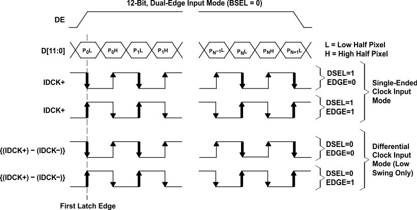
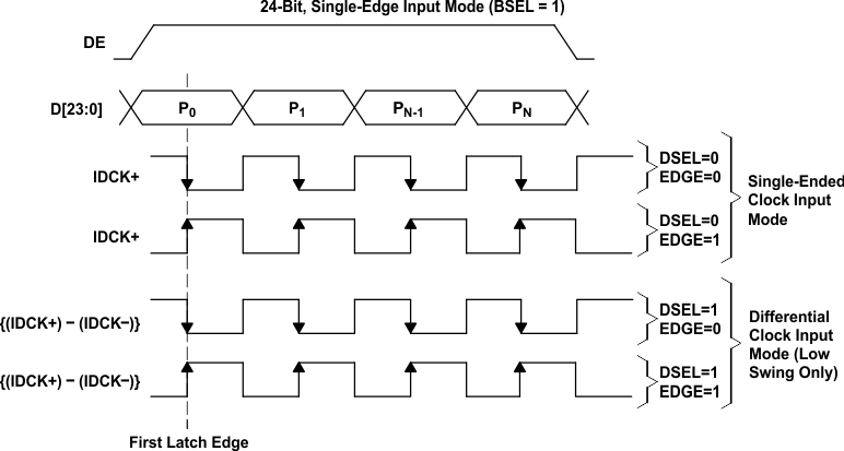
Table 6-1 is a tabular representation of the different modes for the universal graphics controller interface. The 12-bit mode is selected when BSEL=0 and the 24-bit mode when BSEL=1. The 12-bit mode uses dual-edge clocking and the 24-bit mode uses single-edge clocking. The EDGE input is used to control the latching edge in 24-bit mode, or the primary latching edge in 12-bit mode. When EDGE=1, the data input is latched on the rising edge of the input clock; and when EDGE=0, the data input is latched on the falling edge of the input clock. A fully differential input clock is available only in the low-swing mode. Single-ended clocking is not recommended in the low-swing mode as this decreases common-mode noise rejection.
Note that BSEL, DSEL, and EDGE are determined by register CTL_1_MODE when I2C is enabled (ISEL=1) and by input pins when I2C is disabled (ISEL=0).
| VREF | BSEL | EDGE | DSEL | BUS WIDTH | LATCH MODE | CLOCK EDGE | CLOCK MODE |
|---|---|---|---|---|---|---|---|
| 0.55V − 0.9V | 0 | 0 | 0 | 12-bit | Dual-edge | Falling | Differential(1)(2) |
| 0.55V − 0.9V | 0 | 0 | 1 | 12-bit | Dual-edge | Falling | Single-ended |
| 0.55V – 0.9V | 0 | 1 | 0 | 12-bit | Dual-edge | Rising | Differential(1)(2) |
| 0.55V − 0.9V | 0 | 1 | 1 | 12-bit | Dual-edge | Rising | Single-ended |
| 0.55V – 0.9V | 1 | 0 | 0 | 24-bit | Single-edge | Falling | Single-ended |
| 0.55V – 0.9V | 1 | 0 | 1 | 24-bit | Single-edge | Falling | Differential(1)(3) |
| 0.55V – 0.9V | 1 | 1 | 0 | 24-bit | Single-edge | Rising | Single-ended |
| 0.55V – 0.9V | 1 | 1 | 1 | 24-bit | Single-edge | Rising | Differential(1)(3) |
| DVDD | 0 | 0 | X | 12-bit | Dual-edge | Falling | Single-ended(4) |
| DVDD | 0 | 1 | X | 12-bit | Dual-edge | Rising | Single-ended(4) |
| DVDD | 1 | 0 | X | 24-bit | Single-edge | Falling | Single-ended(4) |
| DVDD | 1 | 1 | X | 24-bit | Single-edge | Rising | Single-ended(4) |
 Figure 6-1 Universal Graphics Controller Interface Options for 12-Bit Mode (Graphical Representation)
 Figure 6-2 Universal Graphics Controller Interface Options for 24-Bit Mode (Graphical Representation)
| PIN NAME | P0 | P1 | P2 | |||
|---|---|---|---|---|---|---|
| P0L | P0H | P1L | P1H | P2L | P2H | |
| LOW | HIGH | LOW | HIGH | LOW | HIGH | |
| D11 | G0[3] | R0[7] | G1[3] | R1[7] | G2[3] | R2[7] |
| D10 | G0[2] | R0[6] | G1[2] | R1[6] | G2[2] | R2[6] |
| D9 | G0[1] | R0[5] | G1[1] | R1[5] | G2[1] | R2[5] |
| D8 | G0[0] | R0[4] | G1[0] | R1[4] | G2[0] | R2[4] |
| D7 | B0[7] | R0[3] | B1[7] | R1[3] | B2[7] | R2[3] |
| D6 | B0[6] | R0[2] | B1[6] | R1[2] | B2[6] | R2[2] |
| D5 | B0[5] | R0[1] | B1[5] | R1[1] | B2[5] | R2[1] |
| D4 | B0[4] | R0[0] | B1[4] | R1[0] | B2[4] | R2[0] |
| D3 | B0[3] | G0[7] | B1[3] | G1[7] | B2[3] | G2[7] |
| D2 | B0[2] | G0[6] | B1[2] | G1[6] | B2[2] | G2[6] |
| D1 | B0[1] | G0[5] | B1[1] | G1[5] | B2[1] | G2[5] |
| D0 | B0[0] | G0[4] | B1[0] | G1[4] | B2[0] | G2[4] |
| PIN NAME | P0 | P1 | P2 | PIN NAME | P0 | P1 | P2 | |
|---|---|---|---|---|---|---|---|---|
| D23 | R0[7] | R1[7] | R2[7] | D11 | G0[3] | G1[3] | G2[3] | |
| D22 | R0[6] | R1[6] | R2[6] | D10 | G0[2] | G1[2] | G2[2] | |
| D21 | R0[5] | R1[5] | R2[5] | D9 | G0[1] | G1[1] | G2[1] | |
| D20 | R0[4] | R1[4] | R2[4] | D8 | G0[0] | G1[0] | G2[0] | |
| D19 | R0[3] | R1[3] | R2[3] | D7 | B0[7] | B1[7] | B2[7] | |
| D18 | R0[2] | R1[2] | R2[2] | D6 | B0[6] | B1[6] | B2[6] | |
| D17 | R0[1] | R1[1] | R2[1] | D5 | B0[5] | B1[5] | B2[5] | |
| D16 | R0[0] | R1[0] | R2[0] | D4 | B0[4] | B1[4] | B2[4] | |
| D15 | G0[7] | G1[7] | G2[7] | D3 | B0[3] | B1[3] | B2[3] | |
| D14 | G0[6] | G1[6] | G2[6] | D2 | B0[2] | B1[2] | B2[2] | |
| D13 | G0[5] | G1[5] | G2[5] | D1 | B0[1] | B1[1] | B2[1] | |
| D12 | G0[4] | G1[4] | G2[4] | D0 | B0[0] | B1[0] | B2[0] |