JAJSF33C August 2017 – February 2023 THS3491
PRODUCTION DATA
- 1 特長
- 2 アプリケーション
- 3 概要
- 4 Revision History
- 5 Device Comparison Table
- 6 Pin Configuration and Functions
- 7 Bare Die Information
- 8 Specifications
- 9 Detailed Description
- 10Application and Implementation
- 11Device and Documentation Support
- 12Mechanical, Packaging, and Orderable Information
パッケージ・オプション
メカニカル・データ(パッケージ|ピン)
サーマルパッド・メカニカル・データ
発注情報
6 Pin Configuration and Functions

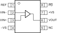
NC - no
internal connection
Figure 6-1 DDA Package, 8-Pin HSOIC
With PowerPAD (Top View)
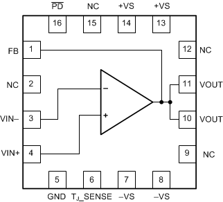
NC - no
internal connection
Figure 6-2 RGT Package, 16-Pin VQFN
With Exposed Thermal Pad (Top View)Table 6-1 Pin Functions
| PIN (1) | TYPE (2) | DESCRIPTION | ||
|---|---|---|---|---|
| NAME | HSOIC | VQFN | ||
| FB | — | 1 | O | Input side feedback pin |
| GND | — | 5 | GND | Ground, PD logic reference on the VQFN-16 (RGT) package |
| NC | 5 | 2, 9, 12, 15 | — | No connect (there is no internal connection). Recommended connection to a heat spreading plane, typically GND. |
| PD | 8 | 16 | I | Amplifier power down: low = amplifier disabled, high (default) = amplifier enabled |
| REF | 1 | — | I | PD logic reference on the SOIC-8 (DDA) package. Typically connected to GND. |
| TJ_SENSE | — | 6 | O | Voltage proportional to die temperature |
| VIN– | 2 | 3 | I | Inverting input |
| VIN+ | 3 | 4 | I | Noninverting input |
| VOUT | 6 | 10, 11 | O | Amplifier output |
| –VS | 4 | 7, 8 | P | Negative power supply |
| +VS | 7 | 13, 14 | P | Positive power supply |
| Thermal pad | — | Thermal pad. Electrically isolated from the device. Recommended connection to a heat spreading plane, typically GND. | ||
(1) Both packages include a backside thermal pad. The thermal pad
can be connected to a heat spreading plane that can be at any voltage because
the device die is electrically isolated from this metal plate. The thermal pad
can also be unused (not connected to any heat spreading plane or voltage) giving
higher thermal impedance.
(2) GND = ground, I = input, O = output, P = power