SLVS029H January 1984 – November 2015 TL499A
PRODUCTION DATA.
- 1 Features
- 2 Applications
- 3 Description
- 4 Revision History
- 5 Pin Configuration and Functions
- 6 Specifications
- 7 Detailed Description
- 8 Application and Implementation
- 9 Power Supply Recommendations
- 10Layout
- 11Device and Documentation Support
- 12Mechanical, Packaging, and Orderable Information
パッケージ・オプション
デバイスごとのパッケージ図は、PDF版データシートをご参照ください。
メカニカル・データ(パッケージ|ピン)
- P|8
- PS|8
サーマルパッド・メカニカル・データ
発注情報
7 Detailed Description
7.1 Overview
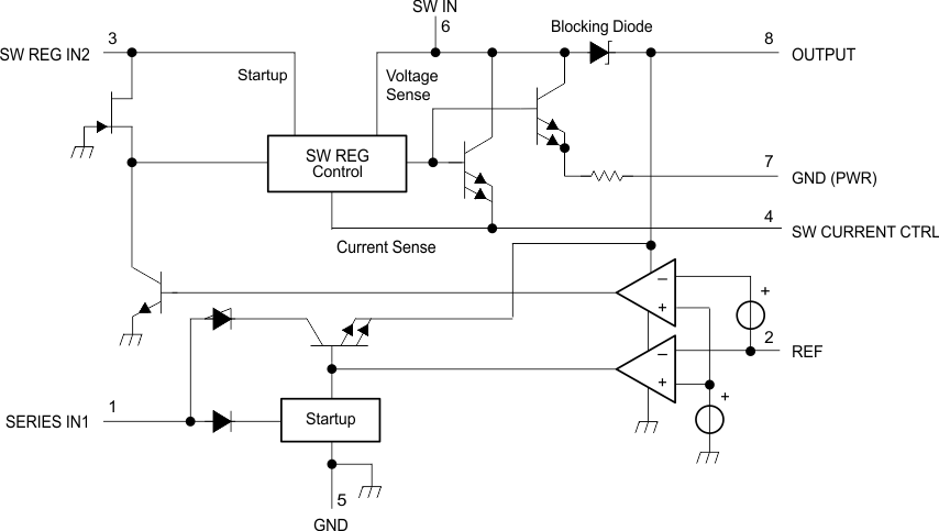
The TL499A provides an adjustable output voltage between 2.9 V and 30 V. The primary power source uses the internal linear regulator to provide the output voltage. When the primary power source is removed, the secondary power source is stepped up using the internal switching regulator to provide the output voltage.
7.2 Functional Block Diagram

7.3 Feature Description
The TL499A has an adjustable output voltage set by feedback provided to REF pin abs an adjustable switching current is set by value of resistor on SW CURRENT CONTROL pin. The lower resistance provides increased switching current.
Dual power supply inputs also provide protection against power faults on the main supply of the TL499A.
7.4 Device Functional Modes
The TL499A has two functional modes:
- Linear voltage regulation when SERIES IN1 supply is present.
- Step-up voltage regulation when SERIES IN1 supply is absent.