JAJSGP1 December   2018 TLV1805

PRODUCTION DATA.  

  1. 特長
  2. アプリケーション
  3. 概要
    1.     Device Images
      1.      P チャネル MOSFET による過電圧保護
      2.      P チャネル MOSFET による逆電流および過電圧保護
  4. 改訂履歴
  5. 概要 (続き)
  6. Pin Configuration and Functions
    1.     Pin Functions
  7. Specifications
    1. 7.1 Absolute Maximum Ratings
    2. 7.2 ESD Ratings
    3. 7.3 Recommended Operating Conditions
    4. 7.4 Thermal Information
    5. 7.5 Electrical Characteristics
    6. 7.6 Switching Characteristics
    7. 7.7 Typical Characteristics
  8. Detailed Description
    1. 8.1 Overview
    2. 8.2 Functional Block Diagram
    3. 8.3 Feature Description
      1. 8.3.1 Rail to Rail Inputs
      2. 8.3.2 Power On Reset
      3. 8.3.3 High Power Push-Pull Output
      4. 8.3.4 Shutdown Function
      5. 8.3.5 Internal Hysteresis
    4. 8.4 Device Functional Modes
      1. 8.4.1 External Hysteresis
        1. 8.4.1.1 Inverting Comparator With Hysteresis
        2. 8.4.1.2 Noninverting Comparator With Hysteresis
  9. Application and Implementation
    1. 9.1 Application Information
    2. 9.2 Typical Applications
      1. 9.2.1 Design Requirements
      2. 9.2.2 Detailed Design Procedure
      3. 9.2.3 Application Curve
      4. 9.2.4 Reverse Current Protection Using MOSFET and TLV1805
        1. 9.2.4.1 Minimum Reverse Current
        2. 9.2.4.2 N-Channel Reverse Current Protection Circuit
          1. 9.2.4.2.1 N-Channel Oscillator Circuit
      5. 9.2.5 P-Channel Reverse Current Protection Circuit
      6. 9.2.6 P-Channel Reverse Current Protection With Overvotlage Protection
      7. 9.2.7 ORing MOSFET Controller
  10. 10Power Supply Recommendations
  11. 11Layout
    1. 11.1 Layout Guidelines
    2. 11.2 Layout Example
  12. 12デバイスおよびドキュメントのサポート
    1. 12.1 ドキュメントのサポート
      1. 12.1.1 関連資料
    2. 12.2 ドキュメントの更新通知を受け取る方法
    3. 12.3 コミュニティ・リソース
    4. 12.4 商標
    5. 12.5 静電気放電に関する注意事項
    6. 12.6 Glossary
  13. 13メカニカル、パッケージ、および注文情報

パッケージ・オプション

メカニカル・データ(パッケージ|ピン)
サーマルパッド・メカニカル・データ
発注情報

ORing MOSFET Controller

The previous reverse current circuits may be combined to create an OR'ing supply controller, utilizing either the P-Channel or N-Channel topologies.

For the previous P-Channel circuit, if no negative input voltages are possible, and the input voltage is below the MOSFET's VGS(MAX) , then D3, D4 and R4 may be eliminated (the D2 anode, U1 pins 2 and 5, and C1 can be directly grounded).

For the N-Channel circuit, the oscillator drive can be shared between the channels, or eliminated if a higher system voltage is available to provide the higher votlage.
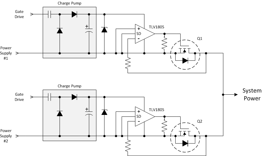
TLV1805 ORing.gifFigure 72. N-Channel OR'ing MOSFET Controller