JAJSI28A October 2019 – August 2020 TPA3139D2
PRODUCTION DATA
- 1 特長
- 2 アプリケーション
- 3 概要
- 4 Revision History
- 5 Pin Configuration and Functions
- 6 Specifications
-
7 Detailed Description
- 7.1 Overview
- 7.2 Functional Block Diagram
- 7.3
Feature Description
- 7.3.1 Analog Gain
- 7.3.2 SD/ FAULT and MUTE Operation
- 7.3.3 PLIMIT
- 7.3.4 Spread Spectrum and De-Phase Control
- 7.3.5 GVDD Supply
- 7.3.6 DC Detect
- 7.3.7 PBTL Select
- 7.3.8 Short-Circuit Protection and Automatic Recovery Feature
- 7.3.9 Over-Temperature Protection (OTP)
- 7.3.10 Over-Voltage Protection (OVP)
- 7.3.11 Under-Voltage Protection (UVP)
- 7.4 Device Functional Modes
-
8 Application and Implementation
- 8.1 Application Information
- 8.2
Typical Applications
- 8.2.1 Design Requirements
- 8.2.2
Detailed Design Procedure
- 8.2.2.1 Ferrite Bead Filter Considerations
- 8.2.2.2 Efficiency: LC Filter Required with the Traditional Class-D Modulation Scheme
- 8.2.2.3 When to Use an Output Filter for EMI Suppression
- 8.2.2.4 Input Resistance
- 8.2.2.5 Input Capacitor, Ci
- 8.2.2.6 BSN and BSP Capacitors
- 8.2.2.7 Differential Inputs
- 8.2.2.8 Using Low-ESR Capacitors
- 8.2.3 Application Performance Curves
- 9 Power Supply Recommendations
- 10Layout
- 11Device and Documentation Support
パッケージ・オプション
メカニカル・データ(パッケージ|ピン)
- RGE|24
サーマルパッド・メカニカル・データ
- RGE|24
発注情報
8.2.2.5 Input Capacitor, Ci
In the typical application, an input capacitor (Ci) is required to allow the amplifier to bias the input signal to the proper dc level for optimum operation. In this case, Ci and the input impedance of the amplifier (Zi) form a high-pass filter with the corner frequency determined in Equation 2.
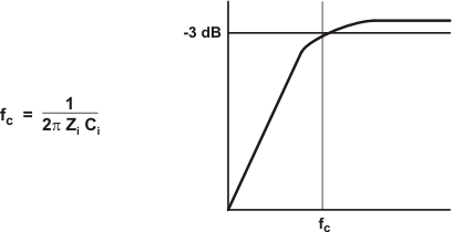
The value of Ci is important, as it directly affects the bass (low-frequency) performance of the circuit. Consider the example where Zi is 20 kΩ (26dB Gain) and the specification calls for a flat bass response down to 20 Hz. Equation 2 is reconfigured as Equation 3.

In this example, Ci is 0.4 µF; so, one would likely choose a value of 0.39 μF as this value is commonly used. A further consideration for this capacitor is the leakage path from the input source through the input network (Ci) and the feedback network to the load. This leakage current creates a dc offset voltage at the input to the amplifier that reduces useful headroom. For this reason, a low-leakage tantalum or ceramic capacitor is the best choice. When polarized capacitors are used, the positive side of the capacitor should face the amplifier input in most applications as the dc level there is held at 3 V, which is likely higher than the source dc level. Note that it is important to confirm the capacitor polarity in the application. Additionally, lead-free solder can create dc offset voltages and it is important to ensure that boards are cleaned properly.