JAJSI28A October 2019 – August 2020 TPA3139D2
PRODUCTION DATA
- 1 特長
- 2 アプリケーション
- 3 概要
- 4 Revision History
- 5 Pin Configuration and Functions
- 6 Specifications
-
7 Detailed Description
- 7.1 Overview
- 7.2 Functional Block Diagram
- 7.3
Feature Description
- 7.3.1 Analog Gain
- 7.3.2 SD/ FAULT and MUTE Operation
- 7.3.3 PLIMIT
- 7.3.4 Spread Spectrum and De-Phase Control
- 7.3.5 GVDD Supply
- 7.3.6 DC Detect
- 7.3.7 PBTL Select
- 7.3.8 Short-Circuit Protection and Automatic Recovery Feature
- 7.3.9 Over-Temperature Protection (OTP)
- 7.3.10 Over-Voltage Protection (OVP)
- 7.3.11 Under-Voltage Protection (UVP)
- 7.4 Device Functional Modes
-
8 Application and Implementation
- 8.1 Application Information
- 8.2
Typical Applications
- 8.2.1 Design Requirements
- 8.2.2
Detailed Design Procedure
- 8.2.2.1 Ferrite Bead Filter Considerations
- 8.2.2.2 Efficiency: LC Filter Required with the Traditional Class-D Modulation Scheme
- 8.2.2.3 When to Use an Output Filter for EMI Suppression
- 8.2.2.4 Input Resistance
- 8.2.2.5 Input Capacitor, Ci
- 8.2.2.6 BSN and BSP Capacitors
- 8.2.2.7 Differential Inputs
- 8.2.2.8 Using Low-ESR Capacitors
- 8.2.3 Application Performance Curves
- 9 Power Supply Recommendations
- 10Layout
- 11Device and Documentation Support
パッケージ・オプション
メカニカル・データ(パッケージ|ピン)
- RGE|24
サーマルパッド・メカニカル・データ
- RGE|24
発注情報
7.3.3 PLIMIT
If selected, the PLIMIT operation limits the output voltage to a level below the supply rail. If the amplifier operates like it is powered by a lower supply voltage, then it limits the output power by voltage clipping. Add a resistor divider from GVDD to ground to set the threshold voltage at the PLIMIT pin.
 Figure 7-1 PLIMIT Circuit Operation
The PLIMIT circuit sets a limit on the output peak-to-peak voltage. The limiting is done by limiting the duty cycle to a fixed maximum value. The limit can be thought of as a "virtual" voltage rail which is lower than the supply connected to PVCC. The "virtual" rail is approximately 5.7 times (with BD mode) and 11.4 times (with 1SPW mode) the voltage at the PLIMIT pin. The output voltage can be used to calculate the maximum output power for a given maximum input voltage and speaker impedance.
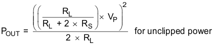
where
- POUT (10%THD) = 1.25 × POUT (unclipped)
- RL is the load resistance.
- RS is the total series resistance including RDS(on), and output filter resistance.
- VP is the peak amplitude, which is limited by "virtual" voltage rail.