SLOS700C January 2011 – April 2016 TPA6139A2
UNLESS OTHERWISE NOTED, this document contains PRODUCTION DATA.
- 1 Features
- 2 Applications
- 3 Description
- 4 Revision History
- 5 Device Comparison Table
- 6 Pin Configuration and Functions
- 7 Specifications
- 8 Parameter Measurement Information
- 9 Detailed Description
- 10Application and Implementation
- 11Power Supply Recommendations
- 12Layout
- 13Device and Documentation Support
- 14Mechanical, Packaging, and Orderable Information
パッケージ・オプション
メカニカル・データ(パッケージ|ピン)
サーマルパッド・メカニカル・データ
発注情報
6 Pin Configuration and Functions
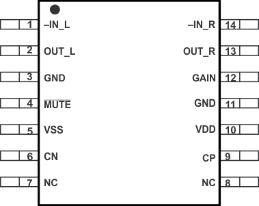
PW Package
14-Pin TSSOP
Top View

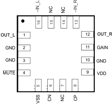
RGT Package
16-Pin VQFN
Top View

Pin Functions
| PIN | TYPE(1) | DESCRIPTION | ||
|---|---|---|---|---|
| NAME | TSSOP | VQFN | ||
| CN | 6 | 6 | I/O | Charge Pump flying capacitor negative connection |
| CP | 9 | 8 | I/O | Charge Pump flying capacitor positive connection |
| GAIN | 12 | 11 | I | Gain set programming pin; connect a resistor to ground. See Table 2 for recommended resistor values |
| GND | 3, 11 | 2, 3, 10 | P | Ground |
| –IN_L | 1 | 16 | I | Negative input, left channel |
| –IN_R | 14 | 13 | I | Negative input, right channel |
| MUTE | 4 | 4 | I | MUTE, active low |
| NC | 7, 8 | 7. 14, 15 | — | No internal connection |
| OUT_L | 2 | 1 | O | Output, left channel |
| OUT_R | 13 | 12 | O | Output, right channel |
| VDD | 10 | 9 | P | Supply voltage, connect to positive supply |
| VSS | 5 | 5 | O | Change Pump negative supply voltage |
(1) I = input, O = output, P = power