SLVSBR1F January 2013 – January 2015 TPD4S214
PRODUCTION DATA.
- 1 Features
- 2 Applications
- 3 Description
- 4 Simplified Schematic
- 5 Revision History
- 6 Pin Configuration and Functions
-
7 Specifications
- 7.1 Absolute Maximum Ratings
- 7.2 ESD Ratings
- 7.3 Recommended Operating Conditions
- 7.4 Thermal Information
- 7.5 Thermal Shutdown
- 7.6 Electrical Characteristics for EN, FLT, DET, D+, D-, VBUS, ID Pins
- 7.7 Electrical characteristics for UVLO / OVLO
- 7.8 Electrical Characteristics for DET Circuits
- 7.9 Electrical Characteristics for OTG Switch
- 7.10 Electrical Characteristics for Current Limit and Short Circuit Protection
- 7.11 Supply Current Consumption
- 7.12 Typical Characteristics
-
8 Detailed Description
- 8.1 Overview
- 8.2 Functional Block Diagram
- 8.3
Feature Description
- 8.3.1 Input Voltage Protection at VBUS from -7 V to 30 V
- 8.3.2 IEC 61000-4-2 Level 4 ESD Protection
- 8.3.3 Low RDS(ON) N-CH FET Switch for High Efficiency
- 8.3.4 Compliant with USB2.0 and USB3.0 OTG spec
- 8.3.5 User Adjustable Current Limit From 250 mA to Beyond 1.2 A
- 8.3.6 Built-in Soft-start
- 8.3.7 Reverse Current Blocking
- 8.3.8 Over Voltage Lock Out for VBUS
- 8.3.9 Under Voltage Lock Out for VOTG_IN
- 8.3.10 Thermal Shutdown and Short Circuit Protection
- 8.3.11 Auto Retry on any Fault; no Latching off States
- 8.3.12 Integrated VBUS Detection Circuit
- 8.3.13 Low Capacitance TVS ESD Clamp for USB2.0 High Speed Data Rate
- 8.3.14 Internal 16ms Startup Delay
- 8.3.15 Space Saving WCSP (12-YFF) Package
- 8.3.16 Inrush Current Protection
- 8.3.17 Input Capacitor (Optional)
- 8.3.18 Output Capacitor (Optional)
- 8.3.19 Current Limit
- 8.3.20 Thermal Shutdown
- 8.3.21 VBUS Detection
- 8.3.22 Test Configuration
- 8.4 Device Functional Modes
- 9 Application and Implementation
- 10Power Supply Recommendations
- 11Layout
- 12Device and Documentation Support
- 13Mechanical, Packaging, and Orderable Information
11 Layout
11.1 Layout Guidelines
- The optimum placement is as close to the connector as possible.
- EMI during an ESD event can couple from the trace being struck to other nearby unprotected traces, resulting in early system failures. Therefore, the PCB designer needs to minimize the possibility of EMI coupling by keeping any unprotected traces away from the protected traces which are between the TVS and the connector.
- Route the protected traces as straight as possible.
- Avoid using VIAs between the connecter and an I/O protection pin on TPD4S214.
- Avoid 90º turns in traces.
- Electric fields tend to build up on corners, increasing EMI coupling.
- Minimize impedance on the path to GND for maximum ESD dissipation.
- The capacitors on VBUS and VOTG_IN should be placed close to their respective pins on TDP4S214.
11.2 Layout Example
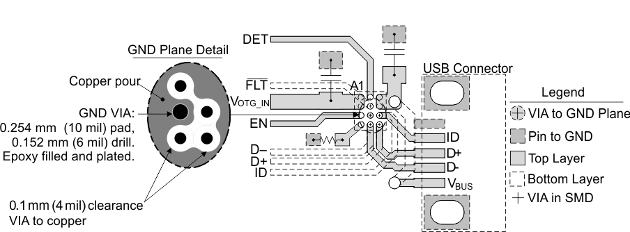 Figure 30. TPD4S214 Layout Example
Successful dissipation of an ESD event is largely dependent on minimizing the impedance along the designated electrical path to ground. For this reason any TVS, including TPD4S214, needs to have the lowest possible impedance to GND. The BGA footprint of this device constrains the path to ground through a VIA in the GND pad of TPD4S214. Due to the "skin effect," maximizing the surface area of the VIA minimizes the impedance of the path to GND. For this reason make both the VIA pad diameter and the VIA drill diameter as large as possible, thus maximizing the surface area of the outside of the VIA surface and the inside of the VIA surface. The GND plane should not be broken in the vicinity of the GND VIA. If possible, attaching the GND VIA to a GND plane on multiple layers minimizes the impedance. The GND VIA should be filled with a non-conductive filler (like epoxy) as opposed to a conductive filler, in order to keep the surface area of the inside of the VIA created by the drill. The GND VIA should be plated over at the SMD pad.