SLVSBR1F January 2013 – January 2015 TPD4S214
PRODUCTION DATA.
- 1 Features
- 2 Applications
- 3 Description
- 4 Simplified Schematic
- 5 Revision History
- 6 Pin Configuration and Functions
-
7 Specifications
- 7.1 Absolute Maximum Ratings
- 7.2 ESD Ratings
- 7.3 Recommended Operating Conditions
- 7.4 Thermal Information
- 7.5 Thermal Shutdown
- 7.6 Electrical Characteristics for EN, FLT, DET, D+, D-, VBUS, ID Pins
- 7.7 Electrical characteristics for UVLO / OVLO
- 7.8 Electrical Characteristics for DET Circuits
- 7.9 Electrical Characteristics for OTG Switch
- 7.10 Electrical Characteristics for Current Limit and Short Circuit Protection
- 7.11 Supply Current Consumption
- 7.12 Typical Characteristics
-
8 Detailed Description
- 8.1 Overview
- 8.2 Functional Block Diagram
- 8.3
Feature Description
- 8.3.1 Input Voltage Protection at VBUS from -7 V to 30 V
- 8.3.2 IEC 61000-4-2 Level 4 ESD Protection
- 8.3.3 Low RDS(ON) N-CH FET Switch for High Efficiency
- 8.3.4 Compliant with USB2.0 and USB3.0 OTG spec
- 8.3.5 User Adjustable Current Limit From 250 mA to Beyond 1.2 A
- 8.3.6 Built-in Soft-start
- 8.3.7 Reverse Current Blocking
- 8.3.8 Over Voltage Lock Out for VBUS
- 8.3.9 Under Voltage Lock Out for VOTG_IN
- 8.3.10 Thermal Shutdown and Short Circuit Protection
- 8.3.11 Auto Retry on any Fault; no Latching off States
- 8.3.12 Integrated VBUS Detection Circuit
- 8.3.13 Low Capacitance TVS ESD Clamp for USB2.0 High Speed Data Rate
- 8.3.14 Internal 16ms Startup Delay
- 8.3.15 Space Saving WCSP (12-YFF) Package
- 8.3.16 Inrush Current Protection
- 8.3.17 Input Capacitor (Optional)
- 8.3.18 Output Capacitor (Optional)
- 8.3.19 Current Limit
- 8.3.20 Thermal Shutdown
- 8.3.21 VBUS Detection
- 8.3.22 Test Configuration
- 8.4 Device Functional Modes
- 9 Application and Implementation
- 10Power Supply Recommendations
- 11Layout
- 12Device and Documentation Support
- 13Mechanical, Packaging, and Orderable Information
7 Specifications
7.1 Absolute Maximum Ratings
over operating free-air temperature range (unless otherwise noted)(1)| MIN | MAX | UNIT | |||
|---|---|---|---|---|---|
| Tstg | Storage temperature range | –40 | 85 | °C | |
| VOTG_IN, ADJ, EN | Input voltage | –0.5 | 7 | V | |
| VBUS | Output voltage to USB connector | –7 | 30 | V | |
| FLT, DET | Output voltage | –0.5 | 7 | V | |
| Input clamp current | VI < 0 | –50 | mA | ||
| IOUT Continuous current through FLT and DET output | 10 | mA | |||
| IGND Continuous current through GND | 100 | mA | |||
| TJ(max) maximum junction temperature | –65 | 150 | °C | ||
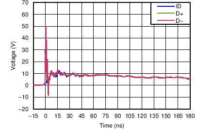
| D+, D-, ID, VBUS pins | IEC 61000-4-2 Contact Discharge at 25°C | ±15 | kV | ||
| D+, D-, ID, VBUS pins | IEC 61000-4-2 Air-gap Discharge at 25°C | ±15 | kV | ||
| D+, D-, ID pins | Peak Pulse Current (tp = 8/20 μs) at 25°C | 7.8 | A | ||
| D+, D-, ID pins | Peak Pulse Power (tp = 8/20 μs) at 25°C | 84 | W | ||
(1) Stresses beyond those listed under Absolute Maximum Ratings may cause permanent damage to the device. These are stress ratings only, which do not imply functional operation of the device at these or any other conditions beyond those indicated under Recommended Operating Conditions. Exposure to absolute-maximum-rated conditions for extended periods may affect device reliability.
7.2 ESD Ratings
| VALUE | UNIT | |||||
|---|---|---|---|---|---|---|
| V(ESD) | Electrostatic discharge | Human body model (HBM), per ANSI/ESDA/JEDEC JS-001, all pins(1) | ±2000 | V | ||
| Charged device model (CDM), per JEDEC specification JESD22-C101, all pins(2) | ±500 | |||||
| IEC 61000-4-2 Contact Discharge | D+, D-, ID, VBUS Pins | ±15000 | V | |||
| IEC 61000-4-2 Air-gap Discharge | ||||||
(1) JEDEC document JEP155 states that 500-V HBM allows safe manufacturing with a standard ESD control process. Pins listed as 2000 V may actually have higher performance.
(2) JEDEC document JEP157 states that 250-V CDM allows safe manufacturing with a standard ESD control process. Pins listed as 500 V may actually have higher performance.
7.3 Recommended Operating Conditions
over operating free-air temperature range (unless otherwise noted)| MIN | TYP | MAX | UNIT | |||
|---|---|---|---|---|---|---|
| TA | Operating free-air temperature | -40 | 85 | °C | ||
| VIH | High-level input voltage EN | 1.2 | V | |||
| VIL | Low-level input voltage EN | 0.4 | V | |||
| tEN | EN ramp rate for proper turn on | Valid ramp rate is between 10 µs and 100 ms, rising and falling | 0.01 | 100 | ms | |
| tUVLO_SLEW | VOTG_IN ramp rate for proper UVLO operation | Valid ramp rate is between 10 µs and 100 ms, rising and falling | 0.01 | 100 | ms | |
| tOVLO_SLEW | VBUS ramp rate for proper OVLO operation | Valid ramp rate is between 10 µs and 100 ms, rising and falling | 0.01 | 100 | ms | |
| TA_VBUS_ATT | Time to detect VBUS device attachment and turn on DET | 200 | ms | |||
7.4 Thermal Information
| THERMAL METRIC(1) | TPD4S214 | UNIT | |
|---|---|---|---|
| YFF | |||
| 12 PINS | |||
| RθJA | Junction-to-ambient thermal resistance | 89.1 | °C/W |
| RθJC(top) | Junction-to-case (top) thermal resistance | 0.5 | |
| RθJB | Junction-to-board thermal resistance | 40.0 | |
| ψJT | Junction-to-top characterization parameter | 3.0 | |
| ψJB | Junction-to-board characterization parameter | 39.0 | |
(1) For more information about traditional and new thermal metrics, see the IC Package Thermal Metrics application report, SPRA953.
7.5 Thermal Shutdown
over operating free-air temperature range (unless otherwise noted)| PARAMETER | TEST CONDITIONS | TYP | MAX | UNIT | |
|---|---|---|---|---|---|
| TSHDN+ | Shutdown temp rising | 141 | ºC | ||
| TSHDN– | Shutdown temp falling | 125 | ºC | ||
| THYST | Thermal-shutdown Hysteresis | 16 | ºC | ||
| PMAX | Maximum power dissipation | VOTG_IN = 5 V, Rload = 5 Ω, EN = 5 V, RADJ = 75 KΩ | 0.16 | W | |
| TJMAX | Junction Temp at max power dissipation | 150 | ºC | ||
7.6 Electrical Characteristics for EN, FLT, DET, D+, D–, VBUS, ID Pins
over operating free-air temperature range (unless otherwise noted)| PARAMETER | TEST CONDITIONS | MIN | TYP | MAX | UNIT | |
|---|---|---|---|---|---|---|
| IIL_EN | EN pin input leakage current | EN = 3.3 V | 1 | µA | ||
| IOL | FLT, DET pin output leakage current | FLT, DET = 3.6 V | 1 | µA | ||
| VOL_FLT | Low-level output voltage FLT | VBUS or VOTG_IN = 5 V or 0 V IOL = 100 µA | 100 | mV | ||
| VOL_DET | Low-level output voltage DET | VBUS and VOTG_IN = 5 V or 0 V IOL = 100 µA | 100 | mV | ||
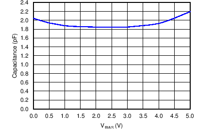
| CEN | Enable capacitance | VBIAS = 1.8 V, f = 1 MHz, 30 mVpp ripple, VOTG_IN = 5 V | 4.5 | pF | ||
| VD | Diode forward voltage D+, D–, ID pins; lower clamp diode | IO = 8 mA | 0.95 | V | ||
| IL_D | Leakage current on D+, D–, ID Pins | D+, D–, ID = 3.3 V | 100 | nA | ||
| ΔCIO | Differential capacitance between the D+, D– lines | VBIAS = 1.8 V, f = 1 MHz, 30 mVpp ripple, VOTG_IN = 5 V | 0.04 | pF | ||
| CIO | Capacitance to GND for the D+, D– lines | VBIAS = 1.8 V, f = 1 MHz, 30 mVpp ripple, VOTG_IN = 5 V | 1.9 | pF | ||
| Capacitance to GND for the ID lines | 1.9 | |||||
| VBR | Breakdown voltage D+, D–, ID pins | Ibr = 1 mA | 6 | V | ||
| Breakdown voltage on VBUS | Ibr = 1 mA | 33 | V | |||
| RDYN | Dynamic on resistance D+, D–, ID clamps | 1 | Ω | |||
7.7 Electrical characteristics for UVLO / OVLO
over operating free-air temperature range (unless otherwise noted)| PARAMETER | TEST CONDITIONS | MIN | TYP | MAX | UNIT | |
|---|---|---|---|---|---|---|
| INPUT UNDER-VOLTAGE LOCKOUT | ||||||
| VUVLO+ | Under-voltage lock-out, input power detected threshold rising | VOTG_IN increasing from 0 V to 5 V, No load on VBUS pin | 3.4 | 3.6 | 3.8 | V |
| VUVLO– | Under-voltage lock-out, input power detected threshold falling | VOTG_IN decreasing from 5 V to 0 V, No load on VBUS pin | 3.0 | 3.2 | 3.5 | V |
| VHYS-UVLO | Hysteresis on UVLO | Δ of VUVLO+ and VUVLO– | 260 | mV | ||
| TRUVLO | Recovery time from UVLO | VOTG_IN increasing from 0V to 5V, No load on VBUS pin; time from VOTG_IN = VUVLO+ to FLT toggles high |
18 | ms | ||
| TRESP_UVLO | Response time for UVLO | VOTG_IN decreasing from 5V to 0V, No load on VBUS pin; time from VOTG_IN = VUVLO– to FLT toggles low |
0.18 | µs | ||
| OUTPUT OVERVOLTAGE LOCKOUT | ||||||
| VOVP+ | OVLO rising threshold | Both VOTG_IN and VBUS increasing from 5 V to 7 V | 5.55 | 6.15 | 6.45 | V |
| VOVP– | OVLO falling threshold | Both VOTG_IN and VBUS decreasing from 7 V to 5 V | 5.4 | 6 | 6.3 | V |
| VHYS-OVP | Hysteresis on OVLO | Δ of VUVLO+ and VUVLO– | 100 | mV | ||
| TROVLO | Recovery time from OVLO | Both VOTG_IN and VBUS decreasing from 7 V to 5 V, VOTG_IN = 5 V; time from VBUS = VOVP– to FLT toggles high |
9 | ms | ||
| TRESP_OVLO | Response time for OVLO | Both VOTG_IN and VBUS increasing from 5 V to 7 V, VOTG_IN = 5 V; time from VBUS = VOVP+ to FLT toggles low |
17 | µs | ||
7.8 Electrical Characteristics for DET Circuits
over operating free-air temperature range (unless otherwise noted)| PARAMETER | TEST CONDITIONS | MIN | TYP | MAX | UNIT | |
|---|---|---|---|---|---|---|
| VBUS_VALID– | Valid VBUS voltage detect | VBUS = 7 V to 0 V | 2.7 | 2.9 | 3 | V |
| VBUS_VALID+ | Valid VBUS voltage detect | VBUS = 0 V to 7 V | 5.3 | 5.4 | 5.6 | V |
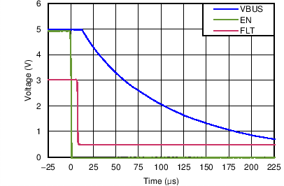
| TDET_DELAY– | VBUS detect propagation delay– | VBUS 0 V to 4 V, 200 ns ramp; VBUS = VBUS_VALID– MIN to DET toggles high | 4.9 | µs | ||
| TDET_DELAY+ | VBUS detect propagation delay+ | VBUS 6 V to 4 V, 200 ns ramp; VBUS = VBUS_VALID+ MAX to DET toggles low | 1.8 | µs | ||
7.9 Electrical Characteristics for OTG Switch
over operating free-air temperature range (unless otherwise noted)| PARAMETER | TEST CONDITIONS | MIN | TYP | MAX | UNIT | ||
|---|---|---|---|---|---|---|---|
| RDS_ON | OTG switch resistance | TA = 25 °C, VBUS = 5 V, IOUT = 100 mA, RADJ = 75 kΩ(1) | 263 | 290 | mΩ | ||
| VDROP | OTG switch voltage drop | VBUS = 5 V, IOUT = 100 mA, RADJ = 75 kΩ | 12.6 | 29 | mV | ||
| IOTG_OFF_30V | Leakage current at 30V | Measured at VOTG_IN | VBUS = 30 V, EN = 5 V, VOTG_IN = 5 V | 6 | µA | ||
| VBUS = 30 V, EN = 5 V, VOTG_IN = 0 V | 11 | nA | |||||
| IOTG_OFF_2V | Leakage current at–2V | VBUS = -2 V, EN = 5 V, VOTG_IN = 5 V | 30 | µA | |||
| IOTG_OFF | Standby Leakage current | VBUS = 0 V, EN = 0 V, VOTG_IN = 5 V | 32 | µA | |||
| VBUS = 5 V, EN = 0 V, VOTG_IN = 0 V | 10 | nA | |||||
| IBUS_REV | Reverse Leakage current | VBUS = 5 V, EN = 5 V, VOTG_IN = 0V | 1 | nA | |||
| VBUS = 5.5 V, EN = 5 V, VOTG_IN = 5 V | 6 | µA | |||||
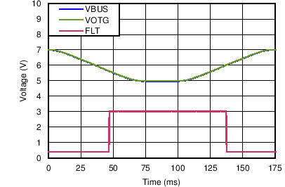
| TON | Turn-ON time | RL = 100 Ω, CL = 1 µF, RADJ = 75 kΩ | 16 | ms | |||
| TOFF_EN | Turn-OFF time | RL = 100 Ω, CL = 1 µF, RADJ = 75 kΩ, toggle EN | 80 | µs | |||
| TOFF_OTG | Turn-OFF time | RL = 100 Ω, CL = 1 µF, RADJ = 75 kΩ, toggle VOTG_IN | 0.5 | µs | |||
| TRISE | Output rise time | RL = 100 Ω, CL = 1 µF, RADJ = 75 kΩ | 137 | µs | |||
| TFALL | Output fall time | RL = 100 Ω, CL = 1 µF, RADJ = 75 kΩ | 1.6 | µs | |||
(1) RDS(ON) is measured at 25°C
7.10 Electrical Characteristics for Current Limit and Short Circuit Protection
over operating free-air temperature range (unless otherwise noted)| PARAMETER | TEST CONDITIONS | MIN | TYP | MAX | UNIT | ||
|---|---|---|---|---|---|---|---|
| IOCP | Current−limit threshold (maximum DC output current IOUT delivered to load) | VOTG_IN = 5 V, RLOAD = 2.0 Ω | RADJ = 226 kΩ(1) | 235 | 245 | 281 | mA |
| RADJ = 75 kΩ(1) | 735 | 792 | 830 | ||||
| RADJ = 62 kΩ(1) | 885 | 959 | 1005 | ||||
| RADJ = 45 kΩ(1) | 1128 | 1200 | 1363 | ||||
| TBLANK | Blanking time after enable | VOTG_IN = 5 V | RL = 1 Ω, CL = 1 µF, RADJ = 75 kΩ |
4 | ms | ||
| TDEGL | Deglitch time while enabled | VOTG_IN = 5 V, RL = 100 Ω, CL = 1 µF, RADJ = 75 kΩ, apply short to ground |
9.4 | ms | |||
| TDET_SC | Response time to short circuit | 10 | µs | ||||
| TREG | Short circuit regulation time | Hiccup pulse width; auto-retry time | 13 | ms | |||
| TOCP | Short circuit over current protection time | Hiccup pulse period | 153 | ms | |||
| VSHORT | Short circuit threshold | 4 | V | ||||
| IINRUSH | Inrush current during a startup | SeeFigure 23 under test configuration | RL = 100 Ω, CL = 22 µF, RADJ = 75 kΩ | 726 | mA | ||
(1) External resistor tolerance is ±1%
7.11 Supply Current Consumption
over operating free-air temperature range (unless otherwise noted)| PARAMETER | TEST CONDITIONS | TYP | MAX | UNIT | ||
|---|---|---|---|---|---|---|
| IVOTG_INON | High-level VOTG_IN operating current consumption | VOTG_IN = 5 V, No load on VBUS, EN = 5 V |
RADJ = 75 kΩ | 162 | 200 | µA |
| RADJ = 226 kΩ | 150 | 200 | µA | |||
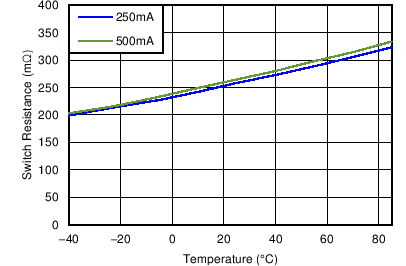
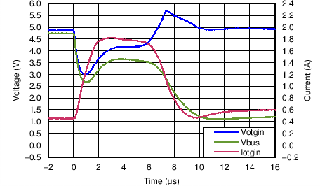
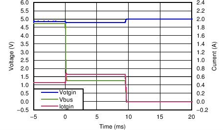
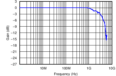
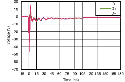
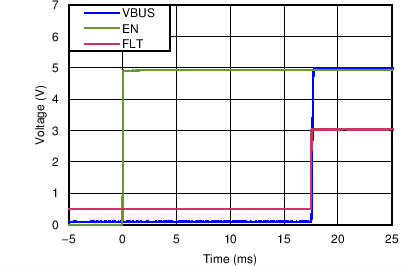
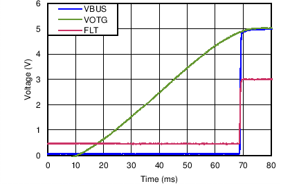
7.12 Typical Characteristics
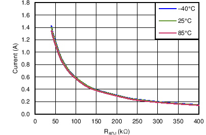
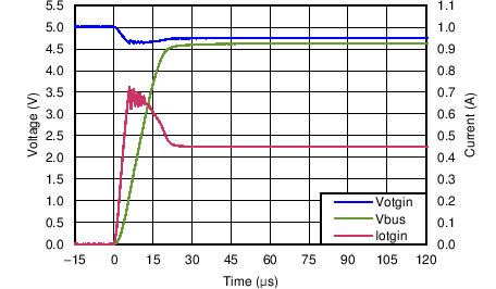
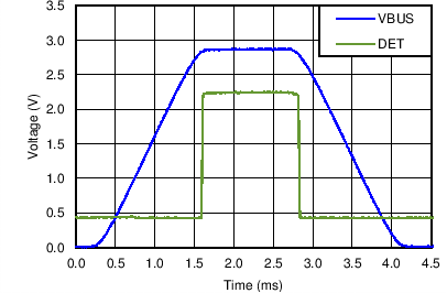
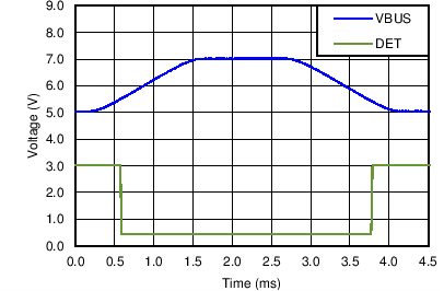
i.
Figure 16. VBUS Valid Detect Upper