SLDS182A August 2010 – July 2015 TPIC7218-Q1
PRODUCTION DATA.
- 1 Device Overview
- 2 Revision History
- 3 Pin Configuration and Functions
-
4 Specifications
- 4.1 Absolute Maximum Ratings
- 4.2 ESD Ratings
- 4.3 Recommended Operating Conditions
- 4.4 Thermal Information
- 4.5 Input Port Electrical Characteristics
- 4.6 PWM Low-Side Driver Electrical Characteristics
- 4.7 Digital Low-Side Driver Electrical Characteristics
- 4.8 High-Side Driver Electrical Characteristics
- 4.9 K-Line Electrical Characteristics
- 4.10 Warning Lamp Electrical Characteristics
- 4.11 Power Supply Electrical Characteristics
- 4.12 SPI Electrical Characteristics
- 4.13 WL_LS Low-Side Switch Output Characteristics
- 4.14 Wheel-Speed High-Side Driver Characteristics
- 4.15 Wheel-Speed Low-Side Driver Characteristics
- 4.16 Wheel-Speed Output Characteristics
- 4.17 RST Output Characteristics
- 4.18 SPI Timing Electrical Characteristics
- 4.19 Power Supply Switching Characteristics
- 4.20 Wheel-Speed Counter Switching Characteristics
- 4.21 HS Driver Switching Characteristics
- 4.22 Digital Low-Side Driver Switching Characteristics
- 4.23 PWM Low-Side Driver Switching Characteristics
- 4.24 K-Line Switching Characteristics
- 4.25 Warning Lamp Switching Characteristics
- 4.26 Watchdog Switching Characteristics
- 4.27 Wheel Speed Interface Switching Characteristics
- 4.28 Wheel-Speed High-Side Driver Switching Characteristics
- 4.29 Wheel-Speed Output Switching Characteristics
- 4.30 Typical Characteristics
-
5 Detailed Description
- 5.1 Overview
- 5.2 Functional Block Diagram
- 5.3
Feature Description
- 5.3.1 Ground Connections
- 5.3.2 Charge Pump
- 5.3.3 Reference Current Generator
- 5.3.4 Wheel-Speed Reference, VREF
- 5.3.5 Faults Common To Most Functional Blocks
- 5.3.6 PWM Low-Side Drivers
- 5.3.7 Digital Low-Side Drivers
- 5.3.8 High-Side Drivers
- 5.3.9 Wheel-Speed Sensing
- 5.3.10 K-Line
- 5.3.11 Warning Lamp Drivers
- 5.3.12 Watchdog Operation
- 5.4 Device Functional Modes
- 5.5 Programming
- 5.6 Register Maps
- 6 Application and Implementation
- 7 Power Supply Recommendations
-
8 Layout
- 8.1
Layout Guidelines
- 8.1.1 Local Grounding Configuration
- 8.1.2 Board Level Grounding Configuration, TPIC7218-Q1 to System Connector
- 8.1.3 VCC3 Bypass Capacitor
- 8.1.4 VDD Bypass Capacitor
- 8.1.5 VBAT and CHP Capacitors
- 8.1.6 Multiple Plane Layer Assignments
- 8.1.7 Duplicate Pad Under TPIC7218-Q1 on All Non-Ground Plane Inner Layers
- 8.1.8 Flooding
- 8.2 Layout Example
- 8.1
Layout Guidelines
- 9 Device and Documentation Support
- 10Mechanical, Packaging, and Orderable Information
パッケージ・オプション
メカニカル・データ(パッケージ|ピン)
- PFP|80
サーマルパッド・メカニカル・データ
- PFP|80
発注情報
6 Application and Implementation
NOTE
Information in the following applications sections is not part of the TI component specification, and TI does not warrant its accuracy or completeness. TI’s customers are responsible for determining suitability of components for their purposes. Customers should validate and test their design implementation to confirm system functionality.
6.1 Application Information
The TPIC7218-Q1 device, as typically used in anti-lock braking systems, requires very few external components; thus, the design is quite simple.
6.2 Typical Application
A simplified application diagram of the TPIC7218-Q1 device Figure 6-1 shows a simplified application diagram.
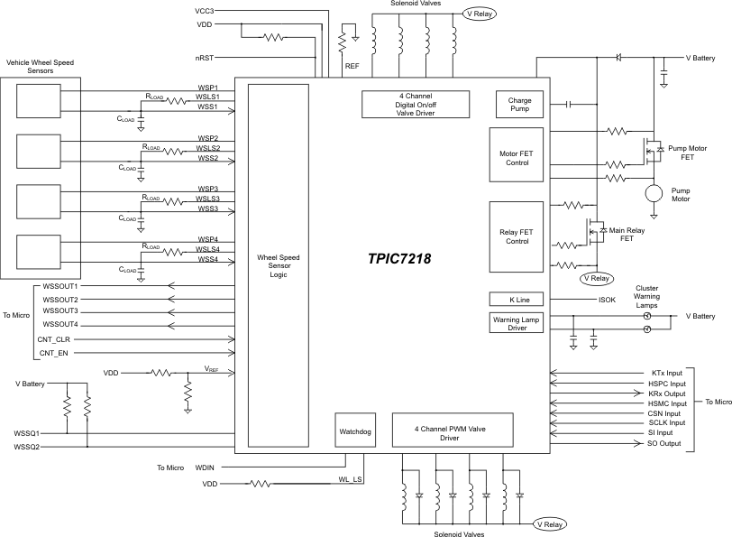 Figure 6-1 Simplified Application Diagram
6.2.1 Design Requirements
The design of the components needed for the wheel speed sensor interface (VREF voltage and RLOAD) is described in Section 5.3.9. The only other major design requirement is in choice of the resistors connected to pins controlling the pump relay (PR) and main relay (MR) FETs as shown in Figure 6-2. The choice of these resistors is described in Section 6.2.2.
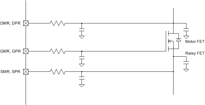 Figure 6-2 xPR and xMR Resistors in Application Diagram
6.2.2 Detailed Design Procedure
The resistor RDMR is to be chosen based on the overcurrent detection value needed for the system relay and pump relay as explained in Section 5.3.8. RSMR resistor value to be chosen to limit the current into the pin in a reverse battery situation - typically in the 1- to 2-kΩ range. See Section 6.2.2.1 for description of the GMR and GPR resistor design procedure.
6.2.2.1 Gatedrive circuit Motor FET
When the pump relay driver at the GPR pin is enabled, it is charged in three different ways. The internal pre-GPR node is shorted to the VBAT supply to give it battery voltage. There are also two current sources that are then enabled at the same time, IDC_GPR and ITRAN_GPR as shown in Figure 6-3. The IDC_GPR current is on any time the pump relay is turned ON. The ITRAN_GPR current source is only enabled for a time tSTGPR after the GPR is turned on. The final voltage will not exceed CHP. The maximum charging time can be obtained from the electrical characteristics table. The turnon time is set by the charging currents with the gate resistor not affecting it significantly. A typical turnon timing characteristic is shown in Figure 6-4, in this case with the IPB 80N06S3L-06 chosen as the pump relay FET.
When the pump relay driver is set to the off state all of the charging paths are disabled and the GPR pin is shorted to GND. The external gate resistance is the primary determinant of the turnoff time. The gate resistor should be sized based on the gate characteristics of the chosen FET and the desired turnoff time. A typical turnoff characteristic with a 10-kΩ resistor is shown in Figure 6-5.
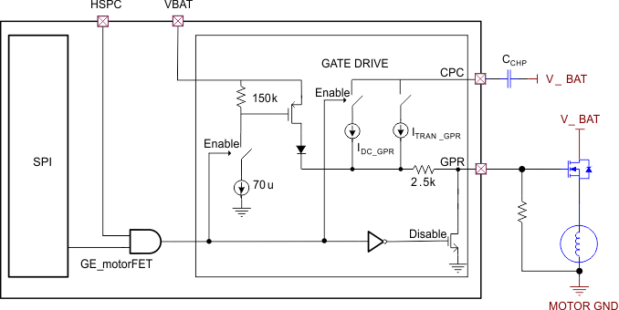 Figure 6-3 Pump Relay Gatedriver Circuit
6.2.2.2 Gatedrive circuit Master Relay FET
The circuit used for the gate drive for the master relay FET is similar to the pump motor FET gatedrive with changes in the drive strength as reflected in the turnon times from the electrical characteristics table. The gate resistor for the master relay FET should be chosen using the same procedure as for the pump motor relay driver.
6.2.3 Application Curves
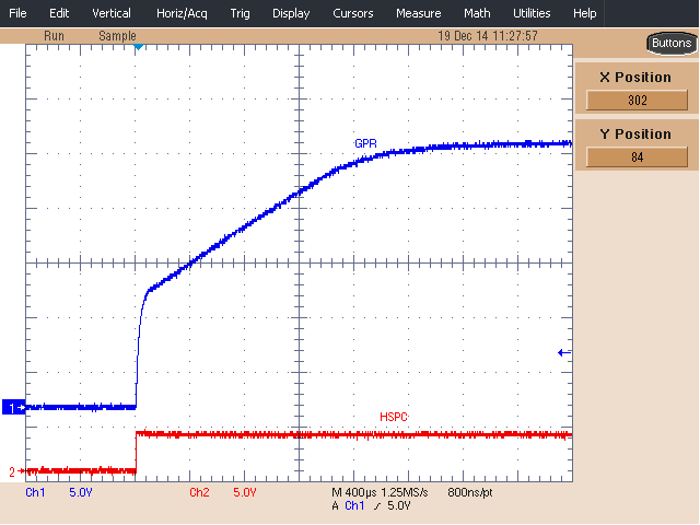 Figure 6-4 Turnon of the FET Gate With a 10-kΩ Gate Resistor.
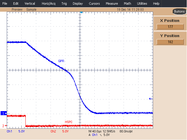 Figure 6-5 Turnon of the FET Gate With a 10-kΩ Gate Resistor.