SLDS182A August 2010 – July 2015 TPIC7218-Q1
PRODUCTION DATA.
- 1 Device Overview
- 2 Revision History
- 3 Pin Configuration and Functions
-
4 Specifications
- 4.1 Absolute Maximum Ratings
- 4.2 ESD Ratings
- 4.3 Recommended Operating Conditions
- 4.4 Thermal Information
- 4.5 Input Port Electrical Characteristics
- 4.6 PWM Low-Side Driver Electrical Characteristics
- 4.7 Digital Low-Side Driver Electrical Characteristics
- 4.8 High-Side Driver Electrical Characteristics
- 4.9 K-Line Electrical Characteristics
- 4.10 Warning Lamp Electrical Characteristics
- 4.11 Power Supply Electrical Characteristics
- 4.12 SPI Electrical Characteristics
- 4.13 WL_LS Low-Side Switch Output Characteristics
- 4.14 Wheel-Speed High-Side Driver Characteristics
- 4.15 Wheel-Speed Low-Side Driver Characteristics
- 4.16 Wheel-Speed Output Characteristics
- 4.17 RST Output Characteristics
- 4.18 SPI Timing Electrical Characteristics
- 4.19 Power Supply Switching Characteristics
- 4.20 Wheel-Speed Counter Switching Characteristics
- 4.21 HS Driver Switching Characteristics
- 4.22 Digital Low-Side Driver Switching Characteristics
- 4.23 PWM Low-Side Driver Switching Characteristics
- 4.24 K-Line Switching Characteristics
- 4.25 Warning Lamp Switching Characteristics
- 4.26 Watchdog Switching Characteristics
- 4.27 Wheel Speed Interface Switching Characteristics
- 4.28 Wheel-Speed High-Side Driver Switching Characteristics
- 4.29 Wheel-Speed Output Switching Characteristics
- 4.30 Typical Characteristics
-
5 Detailed Description
- 5.1 Overview
- 5.2 Functional Block Diagram
- 5.3
Feature Description
- 5.3.1 Ground Connections
- 5.3.2 Charge Pump
- 5.3.3 Reference Current Generator
- 5.3.4 Wheel-Speed Reference, VREF
- 5.3.5 Faults Common To Most Functional Blocks
- 5.3.6 PWM Low-Side Drivers
- 5.3.7 Digital Low-Side Drivers
- 5.3.8 High-Side Drivers
- 5.3.9 Wheel-Speed Sensing
- 5.3.10 K-Line
- 5.3.11 Warning Lamp Drivers
- 5.3.12 Watchdog Operation
- 5.4 Device Functional Modes
- 5.5 Programming
- 5.6 Register Maps
- 6 Application and Implementation
- 7 Power Supply Recommendations
-
8 Layout
- 8.1
Layout Guidelines
- 8.1.1 Local Grounding Configuration
- 8.1.2 Board Level Grounding Configuration, TPIC7218-Q1 to System Connector
- 8.1.3 VCC3 Bypass Capacitor
- 8.1.4 VDD Bypass Capacitor
- 8.1.5 VBAT and CHP Capacitors
- 8.1.6 Multiple Plane Layer Assignments
- 8.1.7 Duplicate Pad Under TPIC7218-Q1 on All Non-Ground Plane Inner Layers
- 8.1.8 Flooding
- 8.2 Layout Example
- 8.1
Layout Guidelines
- 9 Device and Documentation Support
- 10Mechanical, Packaging, and Orderable Information
パッケージ・オプション
メカニカル・データ(パッケージ|ピン)
- PFP|80
サーマルパッド・メカニカル・データ
- PFP|80
発注情報
8 Layout
8.1 Layout Guidelines
8.1.1 Local Grounding Configuration
Route the ground pins 6, 24, 29, 30, 31, 32, 37, 63, 64, 69, 70, 71, 72 and 77 directly inward to pad. Maximize plane area under the TPIC7218-Q1 device to be consistent with PCB design rules. Ensure proper relief features for soldering thermal pad to plated through holes.
Add additional plated through holes as shown in the sketch to minimize loop area for ground return currents. See Figure 8-1 for more information.
8.1.2 Board Level Grounding Configuration, TPIC7218-Q1 to System Connector
Ideally the inner PCB layer under the TPIC7218-Q1 device should be dedicated as plane ground, with direct connection to wiring connector pin to vehicle ground. The layer should cover entire PCB area, with only clearance holes for vias and so forth. No breaks or divisions. See Figure 8-2 for more information.
8.1.3 VCC3 Bypass Capacitor
Place 0402 package bypass capacitor for VCC3 node to ground as close as possible to the TPIC7218-Q1 device, absolute minimum loop width and trace length. Do not connect ground side of capacitor to any plane; tie it directly with top layer trace to pin 6 as shown in Figure 8-3. Close placement, minimum loop area is a priority.
8.1.4 VDD Bypass Capacitor
VDD bypass capacitor needs to be close to the TPIC7218-Q1 device, but not as critical as VCC3 cap. The orientation and location shown in Figure 8-4 is just an example. Connection between capacitor and ground node to be made through a through to the inner ground plane layer.
8.1.5 VBAT and CHP Capacitors
Three capacitors are used for bypassing the VBAT node. Prioritize placing an 0402 as close as possible to pin 59. The other two need to be close but not as critical. Ground capacitors. Capacitor ground needs to be connected to inner plane. The 0805 package is suitable for the other two capacitors.
Two capacitors are used between pin 59 and 60, and as with VBAT node, the 0402 capacitor needs to be as close as possible to the TPIC7218-Q1 device. The 0805 package is suitable for the other capacitor. See Figure 8-5 for more information.
8.1.6 Multiple Plane Layer Assignments
Place components associated with VCC3 (pin 3), VDD (pin 9), VBAT (pin 59), CHP (pin 60), DMR (pin 55), SMR (pin 56), GMR (pin 57), GPR (pin 58), SPR (pin 61) and DPR (pin 62) on top layer. Assign first PCB layer under the top layer as an overall ground plane.
Placing components on top-side of board and assigning first inner layer as ground plane minimizes the path length and loop area for EMC bypassing. See Figure 8-6 for more information.
8.1.7 Duplicate Pad Under TPIC7218-Q1 on All Non-Ground Plane Inner Layers
Duplicate the top layer pad underneath the TPIC7218-Q1 device on all of the inner layers. For the first inner ground plane layer, entire plane is ground except for clearances around holes and unconnected vias. Bottom layer copper pad directly under the TPIC7218-Q1 device is sized and has relief features as required for the thermal slug. See Figure 8-6 for more information.
8.1.8 Flooding
Flooding places copper on all available area, subject to the clearance rules for the manufacture of the PCB. Flooded areas should be connected by vias to the inner ground plane layer. Small, insignificant flooded zones may be left unconnected or deleted from the design.
The additional copper connected to ground augments the effectiveness of the inner ground plane layer by providing parallel paths, and also improves heat sink performance by increasing the thermal mass of the PCB. See Figure 8-7 for more information.
8.2 Layout Example
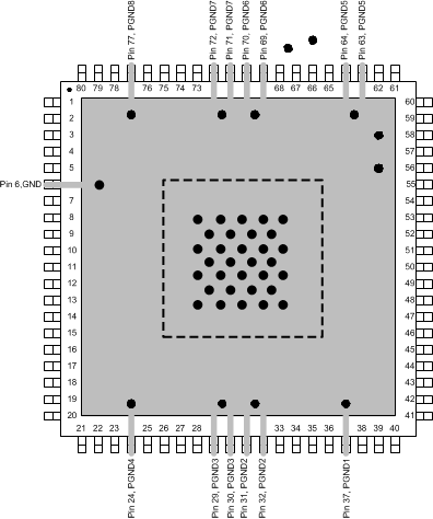 Figure 8-1 Local Grounding Configuration Layout Example
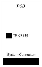 Figure 8-2 Board Level Grounding Configuration, TPIC7218-Q1 to System Connector Layout Example
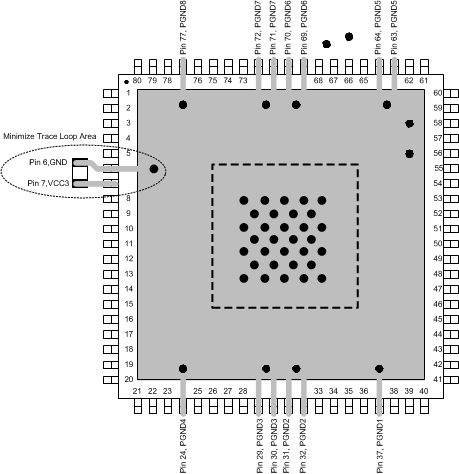 Figure 8-3 VCC3 Bypass Capacitor Layout Example
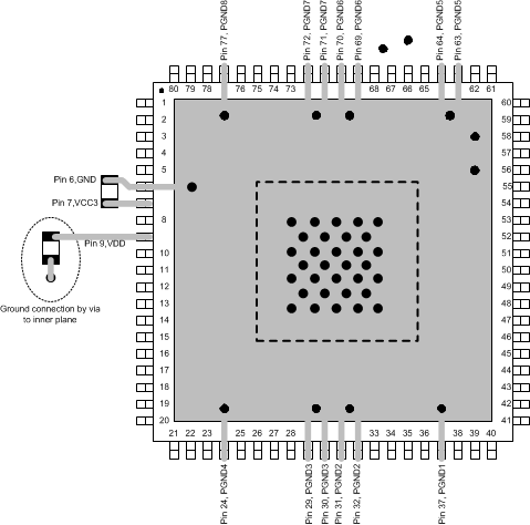 Figure 8-4 VDD Bypass Capacitor Layout Example
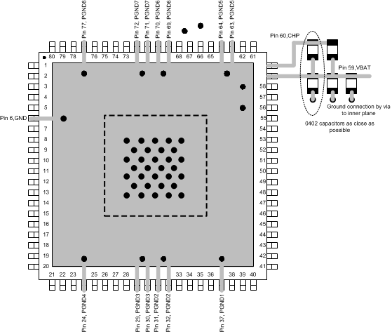 Figure 8-5 VBAT and CHP Capacitors Layout Example
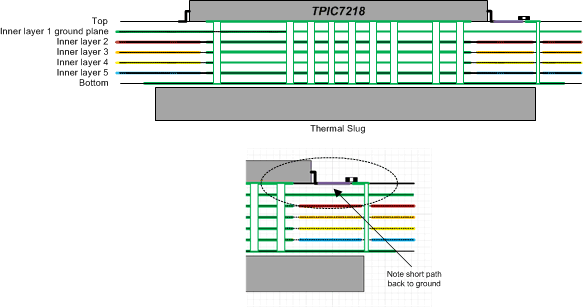 Figure 8-6 Multiple Plane Layer Assignments Layout Example
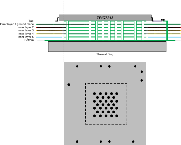 Figure 8-7 Thermal Slug Layout Example