SLVSCL4B August 2014 – September 2014 TPS22994
PRODUCTION DATA.
- 1 Features
- 2 Applications
- 3 Description
- 4 Simplified Schematic
- 5 Revision History
- 6 Device Comparison Table
- 7 Pin Configuration and Functions
- 8 Specifications
-
9 Detailed Description
- 9.1 Overview
- 9.2 Functional Block Diagram
- 9.3
Feature Description
- 9.3.1 Operating Frequency
- 9.3.2 SDA/SCL Pin Configuration
- 9.3.3 Address (ADDx) Pin Configuration
- 9.3.4 On-Delay Control
- 9.3.5 Slew Rate Control
- 9.3.6 Quick Output Discharge (QOD) Control
- 9.3.7 Mode Registers
- 9.3.8 SwitchALL™ Command
- 9.3.9 VDD Supply For I2C Operation
- 9.3.10 Input Capacitor (Optional)
- 9.3.11 Output Capacitor (Optional)
- 9.3.12 I2C Protocol
- 9.4 Device Functional Modes
- 9.5 Register Map
-
10Applications and Implementation
- 10.1 Application Information
- 10.2 Typical Application
- 11Layout
- 12Device and Documentation Support
- 13Mechanical, Packaging, and Orderable Information
パッケージ・オプション
メカニカル・データ(パッケージ|ピン)
- RUK|20
サーマルパッド・メカニカル・データ
- RUK|20
発注情報
9 Detailed Description
9.1 Overview
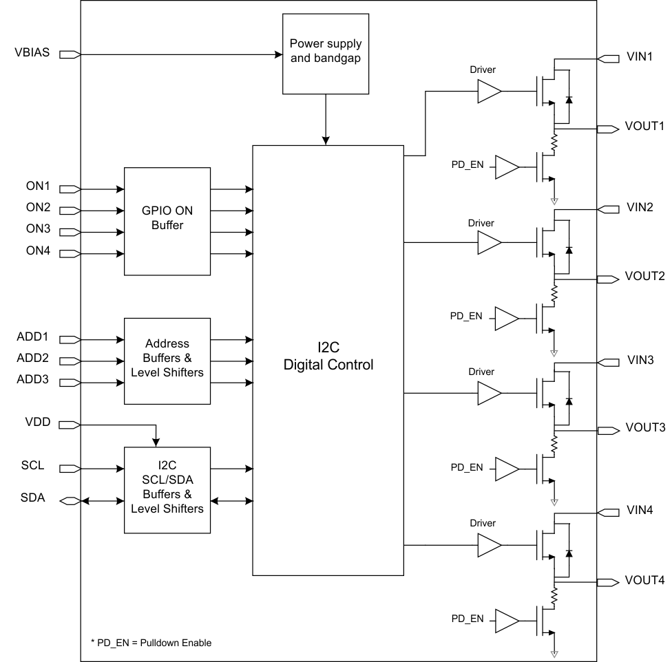
The TPS22994 is a GPIO controllable and I2C programmable, quad-channel load switch. The device comes in a 20-pin QFN package and is designed to handle up to 3.6 V and 1 A per channel (per VINx/VOUTx). The VBIAS pin of the device is designed to interface directly with battery voltages or adapter input voltages as high as 17.2 V. To increase efficiency during standby power, the device implements each channel with an N-channel MOSFET without the use of a chargepump. This allows the quiescent current (IQ,VBIAS) to be much lower than traditional GPIO-based load switches, thus increasing efficiency during standby.
The TPS22994 can be programmed via standard I2C commands. This allows the user to select between 5 slew rates, 4 on-delays, and 4 quick output discharge (QOD) options. The combination of these options allows the user to program the power sequencing for downstream modules via software. Each individual channel can also be controlled (enabling and disabling channels only) via GPIO when I2C communication is not present. The TPS22994 contains a special function called SwitchALLTM that allows multiple devices (either the TPS22993 or TPS22994) to be enabled or disabled synchronously via a single I2C command, allowing the user to switch system power states synchronously.
9.2 Functional Block Diagram
9.3 Feature Description
9.3.1 Operating Frequency
The TPS22994 is designed to be compatible with fast-mode plus and operate up to 1 MHz clock frequency for bus communication. The device is also compatible with standard-mode (100 kHz) and fast-mode (400 kHz). This device can reside on the same bus as high-speed mode (3.4MHz) devices, but the device is not designed to for I2C commands for frequencies greater than 1 MHz. See table below for characteristics of the fast-mode plus, fast-mode, and standard-mode bus speeds.
Table 1. I2C Interface Timing Requirements(1)
| PARAMETER | STANDARD MODE I2C BUS |
FAST MODE I2C BUS |
FAST MODE PLUS (FM+) I2C BUS |
UNIT | ||||
|---|---|---|---|---|---|---|---|---|
| MIN | MAX | MIN | MAX | MIN | MAX | |||
| fscl | I2C clock frequency | 0 | 100 | 0 | 400 | 0 | 1000 | kHz |
| tsch | I2C clock high time | 4 | 0.6 | 0.26 | μs | |||
| tscl | I2C clock low time | 4.7 | 1.3 | 0.5 | μs | |||
| tsp | I2C spike time | 50 | 50 | 50 | ns | |||
| tsds | I2C serial data setup time | 250 | 100 | 50 | ns | |||
| tsdh | I2C serial data hold time | 0 | 0 | 0 | ns | |||
| ticr | I2C input rise time | 1000 | 20 | 300 | 120 | ns | ||
| tbuf | I2C bus free time between Stop and Start | 4.7 | 1.3 | 0.5 | μs | |||
| tsts | I2C Start or repeater Start condition setup time | 4.7 | 0.6 | 0.26 | μs | |||
| tsth | I2C Start or repeater Start condition hold time | 4 | 0.6 | 0.26 | μs | |||
| tsps | I2C Stop condition setup time | 4 | 0.6 | 0.26 | μs | |||
| tvd(data) | Valid data time; SCL low to SDA output valid | 3.45 | 0.3 | 0.9 | 0.45 | μs | ||
| tvd(ack) | Valid data time of ACK condition; ACK signal from SCL low to SDA (out) low | 3.45 | 0.3 | 0.9 | 0.45 | μs | ||
9.3.2 SDA/SCL Pin Configuration
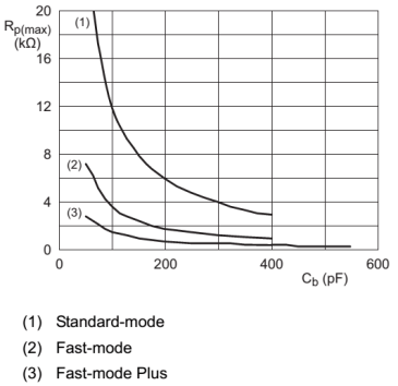
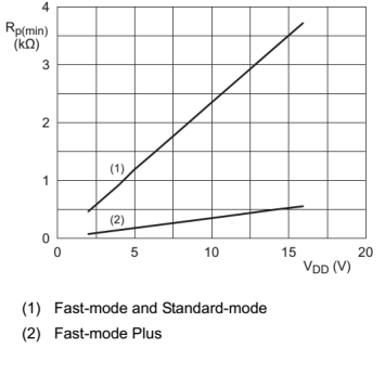
The SDA and SCL pins of the device operate use an open-drain configuration, and therefore, need pull up resistors to communicate on the I2C bus. The graph below shows recommended values for max pull-up resistors (RP) and bus capacitances (Cb) to ensure proper bus communications. The SDA and SCL pins should be pulled up to VDD through an appropriately sized RP based on the graphs below.
9.3.3 Address (ADDx) Pin Configuration
The TPS22994 can be configured with an unique I2C slave addresses by using the ADDx pins. There are 3 ADDx pins that can be tied high to VDD or low to GND (independent of each other) to get up to 7 different slave addresses. The ADDx pins should be tied to GND if the I2C functionality of the device is not to be used. External pull-up resistors for the ADDx are optional as the ADDx inputs are high impedance. The following table shows the ADDx pin tie-offs with their associated slave addresses (assuming an eight bit word, where the LSB is the read/write bit and the device address bits are the 7 MSB bits) :
| Hex Address | ADD3 | ADD2 | ADD1 |
|---|---|---|---|
| E0/E1 | GND | GND | GND |
| E2/E3 | GND | GND | VDD |
| E4/E5 | GND | VDD | GND |
| E6/E7 | GND | VDD | VDD |
| E8/E9 | VDD | GND | GND |
| EA/EB | VDD | GND | VDD |
| EC/ED | VDD | VDD | GND |
| EE | Invalid unique device address. This address is the SwitchALLTM address. |
||
9.3.4 On-Delay Control
Using the I2C interface, the configuration register for each channel can be set for different ON delays for power sequencing. The typical options for delay are as follows (see Switching Characteristics, VBIAS = 7.2 V table):
00 = 11 µs delay (default register value)
01 = 105 µs delay
10 = 330 µs delay
11 = 950 µs delay
It is not recommended to change the delay value for the duration of the delay that is programmed when the channel is enabled (except for ON-delay setting of '00' which requires a minimum of 100µs wait time before changing the setting). This could result in erratic behavior where the output could toggle unintentionally but would eventually recover by the end of the delay time programmed at the time of channel enable.
9.3.5 Slew Rate Control
Using the I2C interface, the configuration register for each channel can be set for different slew rates for inrush current control and power sequencing. The typical options for slew rate are as follows (see Switching Characteristics table for VOUTx rise times):
000 = 1 µs/V
001 = 150 µs/V
010 = 250 µs/V
011 = 460 µs/V (default register value)
100 = 890 µs/V
101 = invalid slew rate
110 = invalid slew rate
111 = reserved
9.3.6 Quick Output Discharge (QOD) Control
Using the I2C interface, the configuration register for each channel can be set for different output discharge resistors. The typical options for QOD are as follows (see Electrical Characteristics table):
00 = 110 Ω
01 = 490 Ω
10 = 951 Ω (default register value)
11 = No QOD (high impedance)
9.3.7 Mode Registers
Using the I2C interface, the mode registers can be programmed to the desired on/off status for each channel. The contents of these registers are copied over to the control registers when a SwitchALL™ command is issued, allowing all channels of the device to transition to their desired output states synchronously. See the I2C Protocol section and the Application Scenario section for more information on how to use the mode registers in conjunction with the SwitchALLTM command.
9.3.8 SwitchALL™ Command
I2C controlled channels can respond to a common slave address. This feature allows multiple load switches on the same I2C bus to respond simultaneously. The SwitchALL™ address is EEh. During a SwitchALL™ command, the lower four bits (bits 0 through 3) of the mode register is copied to the lower four bits (bits 0 through 3) of the control register. The mode register to be invoked is referenced in the body of the SwitchALL™ command. The structure of the SwitchALL™ command is as follows (as shown in Figure 43): <start><SwitchALL™ addr><mode addr><stop>. See the I2C Protocol section and the Application Scenario section for more information on how to use the SwitchALLTM command in conjunction with the mode registers.
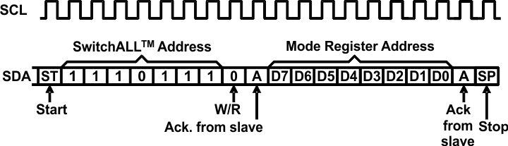 Figure 43. Composition of SwitchALL™ Command
9.3.9 VDD Supply For I2C Operation
The SDA and SCL pins of the device must be pulled up to the VDD voltage of the device for proper I2C bus communication. See Recommended Operating Conditions for VDD operating range.
9.3.10 Input Capacitor (Optional)
To limit the voltage drop on the input supply caused by transient in-rush currents when the switch turns on into a discharged load capacitor or short-circuit, a capacitor needs to be placed between VIN and GND. A 1-µF ceramic capacitor, CIN, placed close to the pins, is usually sufficient. Higher values of CIN can be used to further reduce the voltage drop during high-current application. When switching heavy loads, it is recommended to have an input capacitor about 10 times higher than the output capacitor to avoid excessive voltage drop. For the fastest slew rate setting of the device, a CIN to CL ratio of at least 100 to 1 is recommended to avoid excessive voltage drop.
9.3.11 Output Capacitor (Optional)
Due to the integrated body diode of the NMOS switch, a CIN greater than CL is highly recommended. A CL greater than CIN can cause VOUT to exceed VIN when the system supply is removed. This could result in current flow through the body diode from VOUT to VIN. A CIN to CL ratio of at least 10 to 1 is recommended for minimizing VIN dip caused by inrush currents during startup. For the fastest slew rate setting of the device, a CIN to CL ratio of at least 100 to 1 is recommended to minimize VIN dip caused by inrush currents during startup.
9.3.12 I2C Protocol
The following section will cover the standard I2C protocol used in the TPS22994. In the I2C protocol, the following basic blocks are present in every command (except for the SwitchALLTM command):
- Start/stop bit – marks the beginning and end of each command.
- Slave address – the unique address of the slave device.
- Sub address – this includes the register address and the auto-increment bit.
- Data byte – data being written to the register. Eight bits must always be transferred even if a single bit is being written or read.
- Auto-increment bit – setting this bit to ‘1’ turns on the auto-increment functionality; setting this bit to ‘0’ turns off the auto-increment functionality.
- Write/read bit – this bit signifies if the command being sent will result in reading from a register or writing to a register. Setting this bit to ‘0’ signifies a write, and setting this bit to ‘1’ signifies a read.
- Acknowledge bit – this bit signifies if the master or slave has received the preceding data byte.
9.3.12.1 Start and Stop Bit
In the I2C protocol, all commands contain a START bit and a STOP bit. A START bit, defined by high to low transition on the SDA line while SCL is high, marks the beginning of a command. A STOP bit, defined by low to high transition on the SDA line while SCL is high, marks the end of a command. The START and STOP bits are generated by the master device on the I2C bus. The START bit indicates to other devices that the bus is busy, and some time after the STOP bit the bus is assumed to be free.
9.3.12.2 Auto-increment Bit
The auto-increment feature in the I2C protocol allows users to read from and write to consecutive registers in fewer clock cycles. Since the register addresses are consecutive, this eliminates the need to resend the register address. The I2C core of the device automatically increments the register address pointer by one when the auto-increment bit is set to ‘1’. When this bit is set to ‘0’, the auto-increment functionality is disabled.
9.3.12.3 Write Command
During the write command, the write/read bit is set to ‘0’, signifying that the register in question will be written to. Figure 44 the composition of the write protocol to a single register:
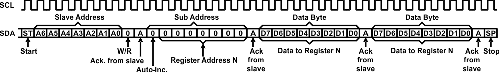 Figure 44. Data Write to a Single Register
Number of clock cycles for single register write: 29
If multiple consecutive registers must be written to, a short-hand version of the write command can be used. Using the auto-increment functionality of I2C, the device will increment the register address after each byte. Figure 45 shows the composition of the write protocol to multiple consecutive registers:
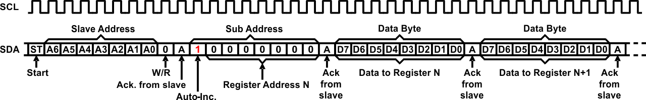 Figure 45. Data Write to Consecutive Registers
Number of clock cycles for consecutive register write: 20 + (Number of registers) x 9
The write command is always ended with a STOP bit after the desired registers have been written to. If multiple non-consecutive registers must be written to, then the format in Figure 44 must be followed.
9.3.12.4 Read Command
During the read command, the write/read bit is set to ‘1’, signifying that the register in question will be read from. However, a read protocol includes a “dummy” write sequence to ensure that the memory pointer in the device is pointing to the correct register that will be read. Failure to precede the read command with a write command may result in a read from a random register. Figure 46 shows the composition of the read protocol to a single register:
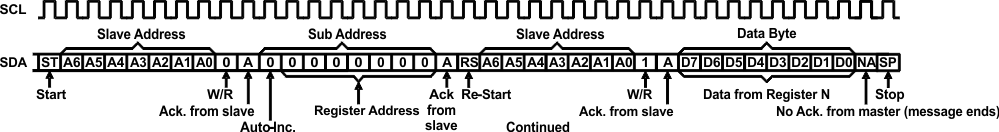 Figure 46. Data Read to a Single Register
Number of clock cycles for single register read: 39
If multiple registers must be read from, a short-hand version of the read command can be used. Using the auto-increment functionality of I2C, the device will increment the register address after each byte. Figure 47 shows the composition of the read protocol to multiple consecutive registers:
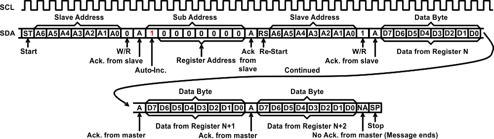 Figure 47. Data Read to Consecutive Registers
Number of clock cycles for consecutive register write: 30 + (Number of registers) x 9
The read command is always ended with a STOP bit after the desired registers have been read from. If multiple non-consecutive registers must be read from, then the format in Figure 46 must be followed.
9.3.12.5 SwitchALLTM Command
The SwitchALLTM command allows multiple devices in the same I2C bus to respond synchronously to the same command from the master. Every TPS22994 device has a shared address which allows for multiple devices to respond or execute a pre-determined action with a single command. Figure 48 shows the composition of the SwitchALLTM command:
Figure 48. SwitchALLTM Command Structure
Number of clock cycles for a SwitchALLTM command: 20
9.4 Device Functional Modes
9.4.1 I2C Control
When power is applied to VBIAS, the device comes up in its default mode of GPIO operation where the channel outputs can be controlled solely via the ON pins. At any time, if SDA and SCL are present and valid, the device can be configured to be controlled via I2C (if in GPIO control) or GPIO (if in I2C control).
The control register (address 05h) can be configured for GPIO or I2C enable on a per channel basis.
9.4.2 GPIO Control
There are four ON pins to enable/disable the four channels. Each ON pin controls the state of the switch by default upon power up. Asserting ON high enables the switch. ON is active high and has a low threshold, making it capable of interfacing with low-voltage signals. The ON pin is compatible with standard GPIO logic threshold. It can be used with any microcontroller with 1.2 V or higher voltage GPIO.
9.5 Register Map
Configuration registers (default register values shown below)
| Channel 1 configuration register (Address: 01h) |
| BIT | B7 | B6 | B5 | B4 | B3 | B2 | B1 | B0 |
| DESCRIPTION | X | ON-DELAY | SLEW RATE | QUICK OUTPUT DISCHARGE | ||||
| DEFAULT | X | 0 | 0 | 0 | 1 | 1 | 1 | 0 |
| Channel 2 configuration register (Address: 02h) |
| BIT | B7 | B6 | B5 | B4 | B3 | B2 | B1 | B0 |
| DESCRIPTION | X | ON-DELAY | SLEW RATE | QUICK OUTPUT DISCHARGE | ||||
| DEFAULT | X | 0 | 0 | 0 | 1 | 1 | 1 | 0 |
| Channel 3 configuration register (Address: 03h) |
| BIT | B7 | B6 | B5 | B4 | B3 | B2 | B1 | B0 |
| DESCRIPTION | X | ON-DELAY | SLEW RATE | QUICK OUTPUT DISCHARGE | ||||
| DEFAULT | X | 0 | 0 | 0 | 1 | 1 | 1 | 0 |
| Channel 4 configuration register (Address: 04h) |
| BIT | B7 | B6 | B5 | B4 | B3 | B2 | B1 | B0 |
| DESCRIPTION | X | ON-DELAY | SLEW RATE | QUICK OUTPUT DISCHARGE | ||||
| DEFAULT | X | 0 | 0 | 0 | 1 | 1 | 1 | 0 |
Control register (default register values shown below)
| Control register (Address: 05h) |
| BIT | B7 | B6 | B5 | B4 | B3 | B2 | B1 | B0 |
| DESCRIPTION | GPIO/I2C ch 4 | GPIO/I2C ch 3 | GPIO/I2C ch 2 | GPIO/I2C ch 1 | ENABLE CH 4 | ENABLE CH 3 | ENABLE CH 2 | ENABLE CH 1 |
| DEFAULT | 0 | 0 | 0 | 0 | 0 | 0 | 0 | 0 |
Mode registers (default register values shown below)
| Mode1 (Address: 06h) |
| BIT | B7 | B6 | B5 | B4 | B3 | B2 | B1 | B0 |
| DESCRIPTION | X | X | X | X | ENABLE CH 4 | ENABLE CH 3 | ENABLE CH 2 | ENABLE CH 1 |
| DEFAULT | X | X | X | X | 0 | 0 | 0 | 0 |
| Mode2 (Address: 07h) |
| BIT | B7 | B6 | B5 | B4 | B3 | B2 | B1 | B0 |
| DESCRIPTION | X | X | X | X | ENABLE CH 4 | ENABLE CH 3 | ENABLE CH 2 | ENABLE CH 1 |
| DEFAULT | X | X | X | X | 0 | 0 | 0 | 0 |
| Mode3 (Address: 08h) |
| BIT | B7 | B6 | B5 | B4 | B3 | B2 | B1 | B0 |
| DESCRIPTION | X | X | X | X | ENABLE CH 4 | ENABLE CH 3 | ENABLE CH 2 | ENABLE CH 1 |
| DEFAULT | X | X | X | X | 0 | 0 | 0 | 0 |
| Mode4 (Address: 09h) |
| BIT | B7 | B6 | B5 | B4 | B3 | B2 | B1 | B0 |
| DESCRIPTION | X | X | X | X | ENABLE CH 4 | ENABLE CH 3 | ENABLE CH 2 | ENABLE CH 1 |
| DEFAULT | X | X | X | X | 0 | 0 | 0 | 0 |
| Mode5 (Address: 0Ah) |
| BIT | B7 | B6 | B5 | B4 | B3 | B2 | B1 | B0 |
| DESCRIPTION | X | X | X | X | ENABLE CH 4 | ENABLE CH 3 | ENABLE CH 2 | ENABLE CH 1 |
| DEFAULT | X | X | X | X | 0 | 0 | 0 | 0 |
| Mode6 (Address: 0Bh) |
| BIT | B7 | B6 | B5 | B4 | B3 | B2 | B1 | B0 |
| DESCRIPTION | X | X | X | X | ENABLE CH 4 | ENABLE CH 3 | ENABLE CH 2 | ENABLE CH 1 |
| DEFAULT | X | X | X | X | 0 | 0 | 0 | 0 |
| Mode7 (Address: 0Ch) |
| BIT | B7 | B6 | B5 | B4 | B3 | B2 | B1 | B0 |
| DESCRIPTION | X | X | X | X | ENABLE CH 4 | ENABLE CH 3 | ENABLE CH 2 | ENABLE CH 1 |
| DEFAULT | X | X | X | X | 0 | 0 | 0 | 0 |
| Mode8 (Address: 0Dh) |
| BIT | B7 | B6 | B5 | B4 | B3 | B2 | B1 | B0 |
| DESCRIPTION | X | X | X | X | ENABLE CH 4 | ENABLE CH 3 | ENABLE CH 2 | ENABLE CH 1 |
| DEFAULT | X | X | X | X | 0 | 0 | 0 | 0 |
| Mode9 (Address: 0Eh) |
| BIT | B7 | B6 | B5 | B4 | B3 | B2 | B1 | B0 |
| DESCRIPTION | X | X | X | X | ENABLE CH 4 | ENABLE CH 3 | ENABLE CH 2 | ENABLE CH 1 |
| DEFAULT | X | X | X | X | 0 | 0 | 0 | 0 |
| Mode10 (Address: 0Fh) |
| BIT | B7 | B6 | B5 | B4 | B3 | B2 | B1 | B0 |
| DESCRIPTION | X | X | X | X | ENABLE CH 4 | ENABLE CH 3 | ENABLE CH 2 | ENABLE CH 1 |
| DEFAULT | X | X | X | X | 0 | 0 | 0 | 0 |
| Mode11 (Address: 10h) |
| BIT | B7 | B6 | B5 | B4 | B3 | B2 | B1 | B0 |
| DESCRIPTION | X | X | X | X | ENABLE CH 4 | ENABLE CH 3 | ENABLE CH 2 | ENABLE CH 1 |
| DEFAULT | X | X | X | X | 0 | 0 | 0 | 0 |
| Mode12 (Address: 11h) |
| BIT | B7 | B6 | B5 | B4 | B3 | B2 | B1 | B0 |
| DESCRIPTION | X | X | X | X | ENABLE CH 4 | ENABLE CH 3 | ENABLE CH 2 | ENABLE CH 1 |
| DEFAULT | X | X | X | X | 0 | 0 | 0 | 0 |