SLVSCL4B August 2014 – September 2014 TPS22994
PRODUCTION DATA.
- 1 Features
- 2 Applications
- 3 Description
- 4 Simplified Schematic
- 5 Revision History
- 6 Device Comparison Table
- 7 Pin Configuration and Functions
- 8 Specifications
-
9 Detailed Description
- 9.1 Overview
- 9.2 Functional Block Diagram
- 9.3
Feature Description
- 9.3.1 Operating Frequency
- 9.3.2 SDA/SCL Pin Configuration
- 9.3.3 Address (ADDx) Pin Configuration
- 9.3.4 On-Delay Control
- 9.3.5 Slew Rate Control
- 9.3.6 Quick Output Discharge (QOD) Control
- 9.3.7 Mode Registers
- 9.3.8 SwitchALL™ Command
- 9.3.9 VDD Supply For I2C Operation
- 9.3.10 Input Capacitor (Optional)
- 9.3.11 Output Capacitor (Optional)
- 9.3.12 I2C Protocol
- 9.4 Device Functional Modes
- 9.5 Register Map
-
10Applications and Implementation
- 10.1 Application Information
- 10.2 Typical Application
- 11Layout
- 12Device and Documentation Support
- 13Mechanical, Packaging, and Orderable Information
パッケージ・オプション
メカニカル・データ(パッケージ|ピン)
- RUK|20
サーマルパッド・メカニカル・データ
- RUK|20
発注情報
8 Specifications
8.1 Recommended Operating Conditions
Over operating free-air temperature range (unless otherwise noted)| MIN | MAX | UNIT | |||
|---|---|---|---|---|---|
| VINx | Input voltage for VIN1, VIN2, VIN3, VIN4 | For VBIAS < 4.6 V | 1.0 | (VBIAS – 1 V) | V |
| For VBIAS ≥ 4.6 V | 1.0 | 3.6 | |||
| VBIAS | Supply voltage for VBIAS | 2.7 | 17.2 | V | |
| VDD | Supply voltage for VDD | 1.62 | 3.6 | V | |
| VADDx | Input voltage for ADD1, ADD2, ADD3 | 0 | VDD | V | |
| VONx | Input voltage for ON1, ON2, ON3, ON4 | 0 | 5 | V | |
| VOUTx | Output voltage for VOUT1, VOUT2, VOUT3, VOUT4 | 0 | VINx | V | |
| CINx | Input capacitor on VIN1, VIN2, VIN3, VIN4 | 1(1) | µF | ||
(1) Refer to application section.
8.2 Absolute Maximum Ratings(1)
Over operating free-air temperature range (unless otherwise noted)| VALUE | UNIT(2) | ||||
|---|---|---|---|---|---|
| MIN | MAX | ||||
| VINx | Input voltage for VIN1, VIN2, VIN3, VIN4 | –0.3 | 4 | V | |
| VBIAS | Supply voltage for VBIAS | –0.3 | 20 | V | |
| VOUTx | Output voltage for VOUT1, VOUT2, VOUT3, VOUT4 | –0.3 | 4 | V | |
| VDD, VSCL, VSDA, VADDx |
Input voltage for VDD, SCL, SDA, ADD1, ADD2, ADD3 | –0.3 | 4 | V | |
| VONx | Input voltage for ON1, ON2, ON3, ON4 | –0.3 | 6 | V | |
| IMAX | Maximum continuous switch current per channel | 1 | A | ||
| TA | Operating free-air temperature(3) | –40 | 85 | °C | |
| TJ | Maximum junction temperature | 125 | °C | ||
| TLEAD | Maximum lead temperature (10-s soldering time) | 300 | °C | ||
(1) Stresses beyond those listed under absolute maximum ratings may cause permanent damage to the device. These are stress ratings only, and functional operation of the device at these or any other conditions beyond those indicated under recommended operating conditions is not implied. Exposure to absolute–maximum–rated conditions for extended periods may affect device reliability.
(2) All voltage values are with respect to network ground pin.
(3) In applications where high power dissipation and/or poor package thermal resistance is present, the maximum ambient temperature may have to be derated. Maximum ambient temperature [TA(max)] is dependent on the maximum operating junction temperature [TJ(max)], the maximum power dissipation of the device in the application [PD(max)], and the junction-to-ambient thermal resistance of the part/package in the application (θJA), as given by the following equation: TA(max) = TJ(max) – (θJA × PD(max))
8.3 Handling Ratings
| MIN | MAX | UNIT | |||
|---|---|---|---|---|---|
| Tstg | Storage temperature | –65 | 150 | °C | |
| ESD(1) | Electrostatic discharge protection | Human-Body Model (HBM)(2) | –2000 | 2000 | V |
| Charged-Device Model (CDM)(3) | –-500 | 500 | V | ||
(1) Electrostatic discharge (ESD) to measure device sensitivity and immunity to damage caused by assembly line electrostatic discharges in to the device.
(2) Level listed above is the passing level per ANSI/ESDA/JEDEC JS-001. JEDEC document JEP155 states that 500V HBM allows safe manufacturing with a standard ESD control process.
(3) Level listed above is the passing level per EIA-JEDEC JESD22-C101. JEDEC document JEP157 states that 250V CDM allows safe manufacturing with a standard ESD control process.
8.4 Thermal Information
| THERMAL METRIC(1)(2) | TPS22994 | UNIT | |
|---|---|---|---|
| RUK | |||
| 20 PINS | |||
| ΘJA | Junction-to-ambient thermal resistance | 46 | °C/W |
| ΘJC(top) | Junction-to-case(top) thermal resistance | 50 | |
| ΘJB | Junction-to-board thermal resistance | 18 | |
| ΨJT | Junction-to-top characterization parameter | 0.7 | |
| ΨJB | Junction-to-board characterization parameter | 18 | |
| ΘJC(bottom) | Junction-to-case(bottom) thermal resistance | 4.2 | |
(1) For more information about traditional and new thermal metrics, see the IC Package Thermal Metrics application report, SPRA953.
(2) For thermal estimates of this device based on PCB copper area, see the TI PCB Thermal Calculator.
8.5 Electrical Characteristics
The specification applies over the operating ambient temperature –40°C ≤ TA ≤ 85°C (Full) (unless otherwise noted). Typical values are for TA = 25°C. VBIAS = 7.2 V (unless otherwise noted).| PARAMETER | TEST CONDITIONS | TA | MIN | TYP | MAX | UNIT | ||
|---|---|---|---|---|---|---|---|---|
| POWER SUPPLIES CURRENTS AND LEAKAGES | ||||||||
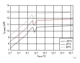
| IQ, VBIAS | Quiescent current for VBIAS (all four channels) | IOUT1,2,3,4 = 0 A, VIN1,2,3,4 = lower of (VBIAS-1 V) or 3.6 V, VON1,2,3,4 = 3.6 V, VDD = 0 V |
VBIAS = 2.7 V | Full | 18.3 | 27.6 | µA | |
| VBIAS = 3.3 V | 18.9 | 28.6 | ||||||
| VBIAS = 4.5 V | 19.4 | 29.9 | ||||||
| VBIAS = 5.2 V | 19.9 | 30.3 | ||||||
| VBIAS = 7.2 V | 21.1 | 33.6 | ||||||
| VBIAS = 10.8 V | 21.2 | 34.8 | ||||||
| VBIAS = 12.6 V | 21.2 | 35.0 | ||||||
| VBIAS = 17.2 V | 21.2 | 35.7 | ||||||
| Quiescent current for VBIAS (single channel) | IOUT1,2,3,4 = 0 A, VIN1 = lower of (VBIAS-1 V) or 3.6 V, VON1 = 3.6 V, VIN2,3,4 = VON2,3,4 = 0 V, VDD = 0 V |
VBIAS = 2.7 V | Full | 8.3 | 16.6 | µA | ||
| VBIAS = 3.3 V | 8.8 | 17.6 | ||||||
| VBIAS = 4.5 V | 9.5 | 18.9 | ||||||
| VBIAS = 5.2 V | 9.9 | 19.6 | ||||||
| VBIAS = 7.2 V | 11.3 | 22.5 | ||||||
| VBIAS = 10.8 V | 11.7 | 23.6 | ||||||
| VBIAS = 12.6 V | 11.7 | 23.8 | ||||||
| VBIAS = 17.2 V | 11.9 | 24.4 | ||||||
| IQ, VDD | Quiescent current for VDD | IOUT1,2,3,4 = 0 A, VIN1,2,3,4 = VON1,2,3,4 = 3.6 V, fSCL = 0 Hz |
VDD = 1.8 V | Full | 0.6 | 1.1 | µA | |
| VDD = 3.6 V | 1.2 | 1.9 | ||||||
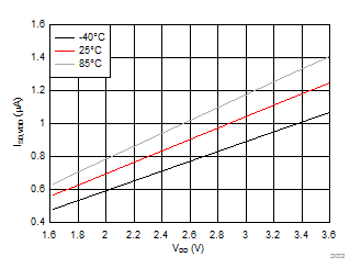
| IDYN, VDD | Average dynamic current for VDD during I2C communication | IOUT1,2,3,4 = 0 A, VIN1,2,3,4 = VON1,2,3,4 = 3.6 V, fSCL = 1 MHz |
VDD = 1.8 V | Full | 7.7 | µA | ||
| VDD = 3.6 V | 19.0 | |||||||
| IDYN, VBIAS | Average dynamic current for VBIAS (all four channels) during I2C communication | IOUT1,2,3,4 = 0 A, VIN1,2,3,4 = lower of (VBIAS-1 V) or 3.6 V, VON1,2,3,4 = 3.6 V, fSCL=1 MHz |
VBIAS = 3.3 V | Full | 65.0 | µA | ||
| VBIAS = 5.2 V | 66.9 | |||||||
| VBIAS = 7.2 V | 68.4 | |||||||
| VBIAS = 10.8 V | 68.5 | |||||||
| VBIAS = 12.6 V | 68.6 | |||||||
| VBIAS = 17.2 V | 69.1 | |||||||
| Average dynamic current for VBIAS (single channel) during I2C communication | IOUT1,2,3,4 = 0 A, VIN1,2,3,4 = lower of (VBIAS-1 V) or 3.6 V, VON1,2,3,4 = 3.6 V, VIN2,3,4 = VON2,3,4 = 0 V, fSCL= 1 MHz |
VBIAS = 3.3 V | Full | 48.0 | µA | |||
| VBIAS = 5.2 V | 58.2 | |||||||
| VBIAS = 7.2 V | 58.9 | |||||||
| VBIAS = 10.8 V | 60.2 | |||||||
| VBIAS = 12.6 V | 60.2 | |||||||
| VBIAS = 17.2 V | 60.7 | |||||||
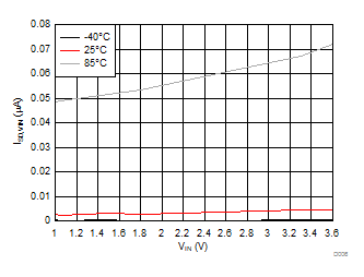
| ISD, VBIAS | Shutdown current for VBIAS (all four channels) | VON1,2,3,4 = 0 V, VOUT1,2,3,4 = 0 V, VDD = 3.6 V, VBIAS = 17.2V |
Full | 6.5 | 12.8 | µA | ||
| ISD, VDD | Shutdown current for VDD | VON1,2,3,4 = 0 V, VOUT1,2,3,4 = 0 V, VDD = 3.6 V |
Full | 1.2 | 1.9 | µA | ||
| ISD, VINx | Shutdown current for VINx | VONx = 0 V, VOUTx = 0 V, VDD = 3.6 V | VINx = 3.6 V | Full | 0.005 | 1.0 | µA | |
| VINx = 3.3 V | 0.004 | 1.0 | ||||||
| VINx = 1.8 V | 0.003 | 0.5 | ||||||
| VINx = 1.5 V | 0.003 | 0.5 | ||||||
| VINx = 1.0 V | 0.003 | 0.5 | ||||||
| IONx | Leakage current for ONx | VONx = 5 V | Full | 0.003 | 0.1 | µA | ||
| IADDx | Leakage current for ADDx | VADDx = 3.6 V | Full | 0.002 | 0.2 | µA | ||
| ISCL | Leakage current for SCL | VSCL = 3.6 V | Full | 0.002 | 0.2 | µA | ||
| ISDA | Leakage current for SDA | VSDA = 3.6 V | Full | 0.002 | 0.2 | µA | ||
| RESISTANCE CHARACTERISTICS | ||||||||
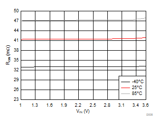
| RON | On-state resistance | VBIAS = 7.2 V, IOUT = –200 mA | VIN = 3.3 V | 25°C | 40.6 | 50.3 | mΩ | |
| Full | 58.5 | |||||||
| VIN = 2.5 V | 25°C | 40.5 | 50.2 | mΩ | ||||
| Full | 58.5 | |||||||
| VIN = 1.8 V | 25°C | 40.5 | 50.1 | mΩ | ||||
| Full | 58.5 | |||||||
| VIN = 1.5 V | 25°C | 40.5 | 50.1 | mΩ | ||||
| Full | 58.5 | |||||||
| VIN = 1.0 V | 25°C | 40.5 | 49.9 | mΩ | ||||
| Full | 58.5 | |||||||
| VBIAS = 5.2 V, IOUT = –200 mA | VIN = 3.3 V | 25°C | 60.4 | 64.0 | mΩ | |||
| Full | 71.0 | |||||||
| VIN = 2.5 V | 25°C | 44.7 | 53.1 | mΩ | ||||
| Full | 65.2 | |||||||
| VIN = 1.8 V | 25°C | 41.5 | 50.3 | mΩ | ||||
| Full | 60.9 | |||||||
| VIN = 1.5 V | 25°C | 40.8 | 50.3 | mΩ | ||||
| Full | 60.5 | |||||||
| VIN = 1.0 V | 25°C | 40.6 | 50.1 | mΩ | ||||
| Full | 60.3 | |||||||
| VBIAS = 3.3 V, IOUT = –200 mA | VIN = 2.3 V | 25°C | 114.2 | 166.0 | mΩ | |||
| Full | 175.0 | |||||||
| VIN = 1.8 V | 25°C | 64.2 | 85.9 | mΩ | ||||
| Full | 94.4 | |||||||
| VIN = 1.5 V | 25°C | 55.4 | 69.5 | mΩ | ||||
| Full | 81.0 | |||||||
| VIN = 1.0 V | 25°C | 48.0 | 57.9 | mΩ | ||||
| Full | 70.0 | |||||||
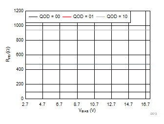
| RPD | Output pulldown resistance | VIN = 3.3 V, VON = 0 V, IOUT = 1 mA, QOD[1:0] = 00 | 25°C | 93 | Ω | |||
| VIN = 3.3 V, VON = 0 V, IOUT = 1 mA, QOD[1:0] = 01 | 25°C | 470 | ||||||
| VIN = 3.3 V, VON = 0 V, IOUT = 1 mA, QOD[1:0] = 10 | 25°C | 940 | ||||||
| VIN = 3.3 V, VON = 0 V, IOUT = 1 mA, QOD[1:0] = 11 | No QOD | |||||||
| THRESHOLD CHARACTERISTICS | ||||||||
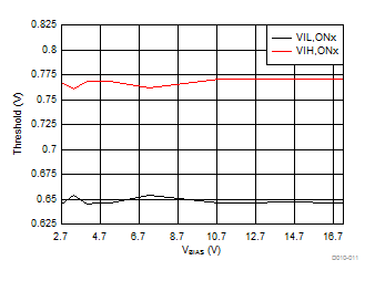
| VIH, ADDx | High-level input voltage for ADDx | Full | 0.7 × VDD | V | ||||
| VIL, ADDx | Low-level input voltage for ADDx | Full | 0.3×VDD | V | ||||
| VIH, ONx | High-level input voltage for ONx | Full | 1.05 | 5 | V | |||
| VIL, ONx | Low-level input voltage for ONx | Full | 0 | 0.4 | V | |||
| VHYS, ONx | Hysteresis for ONx | VBIAS = 2.7 V | 25°C | 107 | mV | |||
| VBIAS = 5.2 V | 105 | |||||||
| VBIAS = 7.2 V | 107 | |||||||
| VBIAS = 10.8 V | 108 | |||||||
| VBIAS = 12.6 V | 109 | |||||||
| VBIAS = 17.2 V | 108 | |||||||
| I2C CHARACTERISTICS | ||||||||
| fSCL(1) | Clock frequency | Full | 1 | MHz | ||||
| tSU, SDA(1) | Setup time for SDA | fSCL = 1 MHz (fast mode plus) | Full | 50 | ns | |||
| tHD, SDA(1) | Hold time for SDA | Full | 0 | ns | ||||
| IOL, SDA | SDA output low current | VOL,SDA = 0.4 V | 25°C | 8 | mA | |||
| VIH, SDA | High-level input voltage for SDA | Full | 0.7 × VDD | VDD | V | |||
| VIH, SCL | High-level input voltage for SCL | Full | 0.7 × VDD | VDD | V | |||
| VIL, SDA | Low-level input voltage for SDA | Full | 0 | 0.3×VDD | V | |||
| VIL, SCL | Low-level input voltage for SCL | Full | 0 | 0.3×VDD | V | |||
(1) Parameter verified by design.
8.6 Switching Characteristics, VBIAS = 7.2 V
Values below are typical values at TA = 25°C. VBIAS = 7.2V (unless otherwise noted).| PARAMETER | TEST CONDITION | VIN VOLTAGE | UNIT | |||||
|---|---|---|---|---|---|---|---|---|
| 3.3 V | 1.8 V | 1.5 V | 1.0 V | |||||
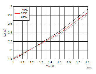
| tON | VOUTx turn-on time | VBIAS = 7.2 V, RL= 10 Ω, CL= 0.1 µF, QOD[1:0] = 10, ON-delay[6:5] = 00 |
Slew rate[4:2] = 000 | 10.2 | 10.0 | 9.9 | 9.9 | µs |
| Slew rate[4:2] = 001 | 220 | 159 | 147 | 124 | ||||
| Slew rate[4:2] = 010 | 380 | 274 | 252 | 213 | ||||
| Slew rate[4:2] = 011 | 674 | 486 | 446 | 377 | ||||
| Slew rate[4:2] = 100 | 1334 | 967 | 888 | 749 | ||||
| tOFF | VOUTx turn-off time | VBIAS = 7.2 V, RL=10 Ω, CL=0.1 µF, QOD[1:0] = 10, ON-delay[6:5] = 00 | 2.5 | 2.5 | 2.5 | 2.5 | µs | |
| tR | VOUTx rise time | VBIAS = 7.2 V, RL= 10 Ω, CL = 0.1 µF, QOD[1:0] = 10, ON-delay[6:5] = 00 |
Slew rate[4:2] = 000 | 1.4 | 0.9 | 0.8 | 0.7 | µs |
| Slew rate[4:2] = 001 | 271 | 178 | 158 | 125 | ||||
| Slew rate[4:2] = 010 | 471 | 309 | 275 | 218 | ||||
| Slew rate[4:2] = 011 | 835 | 549 | 489 | 390 | ||||
| Slew rate[4:2] = 100 | 1674 | 1096 | 976 | 774 | ||||
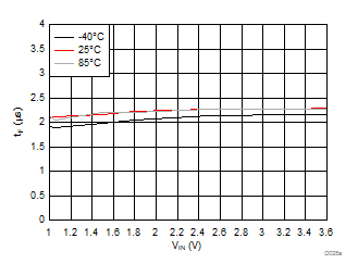
| tF | VOUTx fall time | VBIAS = 7.2 V, RL= 10 Ω, CL= 0.1 µF, QOD[1:0] = 10, ON-delay[6:5] = 00 | 2.3 | 2.3 | 2.3 | 2.3 | µs | |
| tD | VOUTx ON delay time | VBIAS = 7.2 V, RL= 10 Ω, CL= 0.1 µF, QOD[1:0] = 10, Slew rate[6:5] = 000 |
ON delay[4:2] = 00 | 9.6 | 9.6 | 9.6 | 9.6 | µs |
| ON delay[4:2] = 01 | 87 | 87 | 87 | 87 | ||||
| ON delay[4:2] = 10 | 295 | 295 | 295 | 295 | ||||
| ON delay[4:2] = 11 | 846 | 846 | 846 | 846 | ||||
Switching Characteristics, VBIAS = 3.3 V
Values below are typical values at TA = 25°C. VBIAS = 3.3 V (unless otherwise noted).| PARAMETER | TEST CONDITION | VIN VOLTAGE | UNIT | ||||
|---|---|---|---|---|---|---|---|
| 1.8V | 1.5V | 1.0V | |||||
| tON | VOUTx turn-on time | VBIAS = 3.3 V, RL=10 Ω, CL=0.1 µF, QOD[1:0] = 10, ON-delay[6:5] = 00 |
Slew rate[4:2] = 000 | 8.4 | 8.3 | 8.1 | µs |
| Slew rate[4:2] = 001 | 165 | 152 | 129 | ||||
| Slew rate[4:2] = 010 | 283 | 260 | 221 | ||||
| Slew rate[4:2] = 011 | 502 | 460 | 389 | ||||
| Slew rate[4:2] = 100 | 997 | 915 | 773 | ||||
| tOFF | VOUTx turn-off time | VBIAS = 3.3 V, RL=10 Ω, CL=0.1 µF, QOD[1:0] = 10, ON-delay[6:5] = 00 | 2.5 | 2.6 | 2.8 | µs | |
| tR | VOUTx rise time | VBIAS = 3.3 V, RL=10 Ω, CL=0.1 µF, QOD[1:0] = 10, ON-delay[6:5] = 00 |
Slew rate[4:2] = 000 | 2.8 | 2.4 | 1.8 | µs |
| Slew rate[4:2] = 001 | 184 | 163 | 128 | ||||
| Slew rate[4:2] = 010 | 318 | 283 | 224 | ||||
| Slew rate[4:2] = 011 | 565 | 501 | 398 | ||||
| Slew rate[4:2] = 100 | 1126 | 1002 | 791 | ||||
| tF | VOUTx fall time | VBIAS = 3.3 V, RL=10 Ω, CL= 0.1 µF, QOD[1:0] = 10, ON-delay[6:5] = 00 | 2.2 | 2.2 | 2.1 | µs | |
| tD | VOUTx ON delay time | VBIAS = 3.3 V, RL=10 Ω, CL=0.1 µF, QOD[1:0] = 10, Slew rate[6:5] = 000 |
ON delay[4:2] = 00 | 7.3 | 7.3 | 7.3 | µs |
| ON delay[4:2] = 01 | 89 | 89 | 89 | ||||
| ON delay[4:2] = 10 | 296 | 296 | 296 | ||||
| ON delay[4:2] = 11 | 846 | 846 | 846 | ||||
A. Rise and fall times of the control signal is 100 ns.
B. All switching measurements are done using GPIO control only.
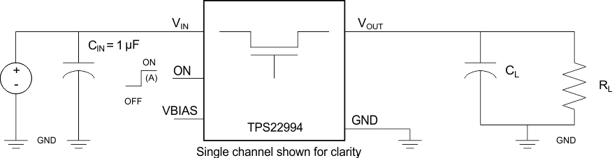
Figure 1. Test Circuit
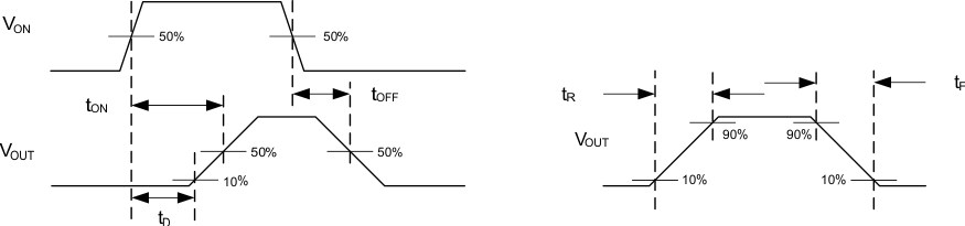 Figure 2. tON/tOFF Waveforms
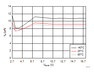
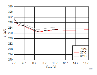
8.7 Typical Characteristics
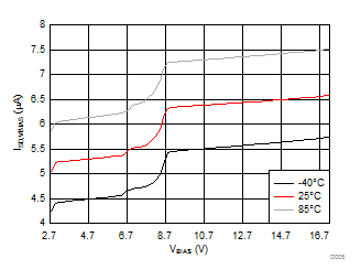
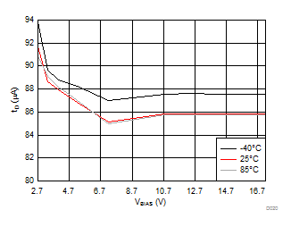
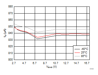
| VBIAS = 7.2 V | VINx = 3.6 V | |
| VINx = lower of (VBIAS-1V) or 3.6 V | VDD = 3.6 V | |
| VINx = lower of (VBIAS-1V) or 3.6 V | VDD = 3.6 V | |
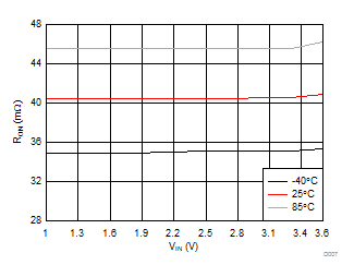
| VBIAS = 7.2 V | IOUT = 200 mA | |
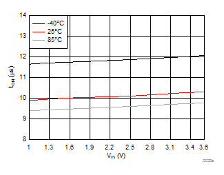
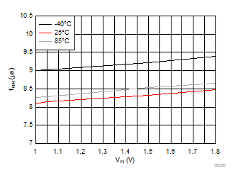
| TA = 25°C | ||
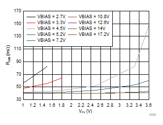
| VINx = lower of (VBIAS-1 V) or 3.6 V | TA = 25°C | |
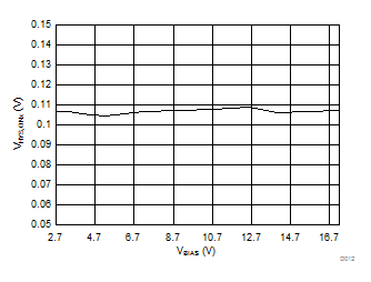
| VBIAS = 7.2 V | VDD = 3.6 V | RL = 10 Ω |
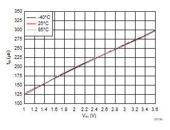
| Slew rate[4:2] = 000 | ||
| VBIAS = 7.2 V | VDD = 3.6 V | RL = 10 Ω |
| Slew rate[4:2] = 001 | ||
| VBIAS = 7.2 V | VDD = 3.6 V | RL = 10 Ω |
| Slew rate[4:2] = 010 | ||
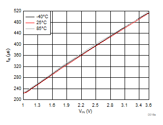
| VBIAS = 7.2 V | VDD = 3.6 V | RL = 10 Ω |
| Slew rate[4:2] = 011 | ||
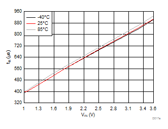
| VBIAS = 7.2 V | VDD = 3.6 V | RL = 10 Ω |
| Slew rate[4:2] = 100 | ||
| ON-delay[6:5] = 00 | VDD = 3.6 V | RL = 10 Ω |
| ON-delay[6:5] = 10 V | VDD = 3.6 V | RL = 10 Ω |
| VBIAS = 7.2 V | VDD = 3.6 V | RL = 10 Ω |
| Slew rate[4:2] = 000 | ||
| VBIAS = 7.2 V | VDD = 3.6 V | RL = 10 Ω |
| Slew rate[4:2] = 001 | ||
A.
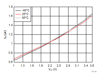
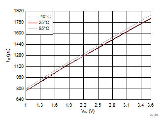
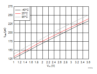
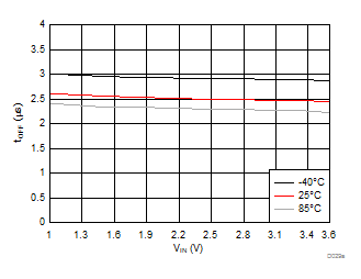
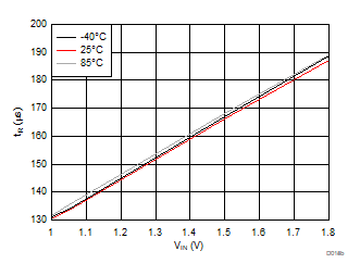
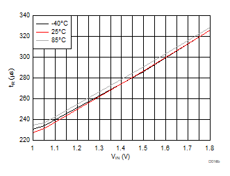
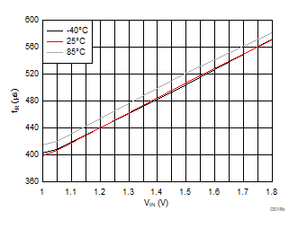
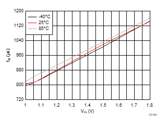
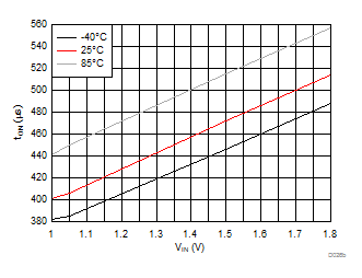
Figure 33. tON vs. VIN
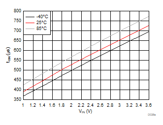
| VBIAS = 7.2 V | VDD = 3.6 V | RL = 10 Ω |
| Slew rate[4:2] = 010 | ||
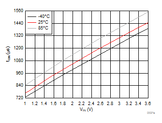
| VBIAS = 7.2 V | VDD = 3.6 V | RL = 10 Ω |
| Slew rate[4:2] = 011 | ||
| VBIAS = 7.2 V | VDD = 3.6 V | RL = 10 Ω |
| Slew rate[4:2] = 100 | ||
| VBIAS = 7.2 V | VDD = 3.6 V | RL = 10 Ω |
| VBIAS = 7.2 V | VDD = 3.6 V | RL = 10 Ω |
| VBIAS = 7.2 V | VINx = 3.6 V | |
| VINx = lower of (VBIAS-1V) or 3.6 V | VDD = 3.6 V | |
| VBIAS = 7.2 V | VDD = 3.6 V | |
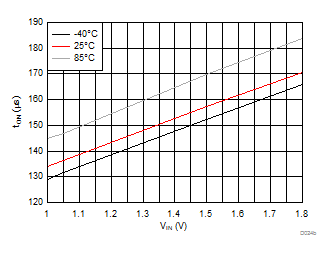
| VBIAS = 7.2 V | IOUT = 1 A | |
| VINx = lower of (VBIAS-1 V) or 3.6 V | TA = 25°C | |
| TA = 25°C | ||
| VBIAS = 3.3 V | VDD = 3.6 V | RL = 10 Ω |
| Slew rate[4:2] = 000 | ||
| VBIAS = 3.3 V | VDD = 3.6 V | RL = 10 Ω |
| Slew rate[4:2] = 001 | ||
| VBIAS = 3.3 V | VDD = 3.6 V | RL = 10 Ω |
| Slew rate[4:2] = 010 | ||
| VBIAS = 3.3 V | VDD = 3.6 V | RL = 10 Ω |
| Slew rate[4:2] = 011 | ||
| VBIAS = 3.3 V | VDD = 3.6 V | RL = 10 Ω |
| Slew rate[4:2] = 100 | ||
| ON-delay[6:5] = 01 | VDD = 3.6 V | RL = 10 Ω |
| ON-delay[6:5] = 11 | VDD = 3.6 V | RL = 10 Ω |
| VBIAS = 3.3 V | VDD = 3.6 V | RL = 10 Ω |
| Slew rate[4:2] = 000 | ||
| VBIAS = 3.3 V | VDD = 3.6 V | RL = 10 Ω |
| Slew rate[4:2] = 001 | ||
| VBIAS = 3.3 V | VDD = 3.6 V | RL = 10 Ω |
| Slew rate[4:2] = 010 | ||
| VBIAS = 3.3 V | VDD = 3.6 V | RL = 10 Ω |
| Slew rate[4:2] = 011 | ||
| VBIAS = 3.3 V | VDD = 3.6 V | RL = 10 Ω |
| Slew rate[4:2] = 100 | ||
| VBIAS = 3.3 V | VDD = 3.6 V | RL = 10 Ω |
| VBIAS = 3.3 V | VDD = 3.6 V | RL = 10 Ω |