JAJSEJ1B november   2017  – july 2020 TPS254900A-Q1

PRODUCTION DATA  

  1.   1
  2. 特長
  3. アプリケーション
  4. 概要
  5. Revision History
  6. Pin Configuration and Functions
    1.     7
  7. Specifications
    1. 6.1 Absolute Maximum Ratings
    2. 6.2 ESD Ratings
    3. 6.3 Recommended Operating Conditions
    4. 6.4 Thermal Information
    5. 6.5 Electrical Characteristics
    6. 6.6 Switching Characteristics
    7. 6.7 Typical Characteristics
  8. Parameter Measurement Information
  9. Detailed Description
    1. 8.1 Overview
    2. 8.2 Functional Block Diagram
    3. 8.3 Feature Description
      1. 8.3.1  FAULT Response
      2. 8.3.2  Cable Compensation
        1. 8.3.2.1 Design Procedure
      3. 8.3.3  D+ and D– Protection
      4. 8.3.4  VBUS OVP Protection
      5. 8.3.5  Output and D+ or D– Discharge
      6. 8.3.6  Port Power Management (PPM)
        1. 8.3.6.1 Benefits of PPM
        2. 8.3.6.2 PPM Details
        3. 8.3.6.3 Implementing PPM in a System With Two Charging Ports (CDP and SDP1)
      7. 8.3.7  Overcurrent Protection
      8. 8.3.8  Undervoltage Lockout
      9. 8.3.9  Thermal Sensing
      10. 8.3.10 Current-Limit Setting
    4. 8.4 Device Functional Modes
      1. 8.4.1 Device Truth Table (TT)
      2. 8.4.2 USB BC1.2 Specification Overview
      3. 8.4.3 Standard Downstream Port (SDP) Mode — USB 2.0 and USB 3.0
      4. 8.4.4 Charging Downstream Port (CDP) Mode
      5. 8.4.5 Client Mode
      6. 8.4.6 High-Bandwidth Data-Line Switch
  10. Application and Implementation
    1. 9.1 Application Information
    2. 9.2 Typical Application
      1. 9.2.1 Design Requirements
      2. 9.2.2 Detailed Design Procedure
        1. 9.2.2.1 Input Capacitance
        2. 9.2.2.2 Output Capacitance
        3. 9.2.2.3 BIAS Capacitance
        4. 9.2.2.4 Output and BIAS TVS
      3. 9.2.3 Application Curves
  11. 10Power Supply Recommendations
  12. 11Layout
    1. 11.1 Layout Guidelines
    2. 11.2 Layout Example
  13. 12Device and Documentation Support
    1. 12.1 Device Support
    2. 12.2 Documentation Support
      1. 12.2.1 Related Documentation
    3. 12.3 ドキュメントの更新通知を受け取る方法
    4. 12.4 サポート・リソース
    5. 12.5 Trademarks
    6. 12.6 静電気放電に関する注意事項
    7. 12.7 用語集
  14. 13Mechanical, Packaging, and Orderable Information

パッケージ・オプション

デバイスごとのパッケージ図は、PDF版データシートをご参照ください。

メカニカル・データ(パッケージ|ピン)
  • RVC|20
サーマルパッド・メカニカル・データ
発注情報

Client Mode

The TPS254900A-Q1 device integrates client mode as shown in Figure 8-6. The internal power switch is OFF to block current flow from OUT to IN, and the signal switches are ON. This mode can be used for software upgrades from the USB port.
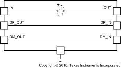
GUID-EACC769B-9D31-4831-A6A9-0514DC706AF0-low.gifFigure 8-6 Client-Mode Equivalent Circuit

Passing the IEC 61000-4-2 test for DP_IN and DM_IN requires connecting a discharge resistor to OUT during USB 2.0 high-speed enumeration. In client mode, because the power switch is OFF, OUT must be 5 V so that the device can work normally (usually powered by an external downstream USB port). If the OUT voltage is low, the communication may not work properly.