JAJSHY1E September 2019 – March 2022 TPS25840-Q1 , TPS25842-Q1
PRODUCTION DATA
- 1 特長
- 2 アプリケーション
- 3 概要
- 4 Revision History
- 5 概要 (続き)
- 6 Device Comparison Table
- 7 Pin Configuration and Functions
- 8 Specifications
- 9 Parameter Measurement Information
-
10Detailed Description
- 10.1 Overview
- 10.2 Functional Block Diagram
- 10.3
Feature Description
- 10.3.1 Buck Regulator
- 10.3.2 Enable/UVLO
- 10.3.3 Switching Frequency and Synchronization (RT/SYNC)
- 10.3.4 Spread-Spectrum Operation
- 10.3.5 VCC, VCC_UVLO
- 10.3.6 Minimum ON-time, Minimum OFF-time
- 10.3.7 Internal Compensation
- 10.3.8 Bootstrap Voltage (BOOT)
- 10.3.9 RSNS, RSET, RILIMIT and RIMON
- 10.3.10 Overcurrent and Short Circuit Protection
- 10.3.11 Overvoltage, IEC and Short-to-Battery Protection
- 10.3.12 Cable Compensation
- 10.3.13 USB Port Control
- 10.3.14 FAULT Response
- 10.3.15 USB Specification Overview
- 10.3.16 Device Power Pins (IN, CSN/OUT, and PGND)
- 10.3.17 Thermal Shutdown
- 10.4 Device Functional Modes
-
11Application and Implementation
- 11.1 Application Information
- 11.2
Typical Application
- 11.2.1 Design Requirements
- 11.2.2
Detailed Design Procedure
- 11.2.2.1 Output Voltage
- 11.2.2.2 Switching Frequency
- 11.2.2.3 Inductor Selection
- 11.2.2.4 Output Capacitor Selection
- 11.2.2.5 Input Capacitor Selection
- 11.2.2.6 Bootstrap Capacitor Selection
- 11.2.2.7 VCC Capacitor Selection
- 11.2.2.8 Enable and Under Voltage Lockout Set-Point
- 11.2.2.9 Current Limit Set-Point
- 11.2.2.10 Cable Compensation Set-Point
- 11.2.2.11 FAULT Resistor Selection
- 11.2.3 Application Curves
- 12Power Supply Recommendations
- 13Layout
- 14Device and Documentation Support
- 15Mechanical, Packaging, and Orderable Information
パッケージ・オプション
メカニカル・データ(パッケージ|ピン)
- RHB|32
サーマルパッド・メカニカル・データ
- RHB|32
発注情報
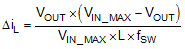
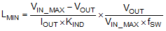
11.2.2.3 Inductor Selection
The most critical parameters for the inductor are the inductance, saturation current and the rated current. The inductance is based on the desired peak-to-peak ripple current ΔiL. Because the ripple current increases with the input voltage, the maximum input voltage is always used to calculate the minimum inductance LMIN. Use Equation 10 to calculate the minimum value of the output inductor. KIND is a coefficient that represents the amount of inductor ripple current relative to the maximum output current of the device. A reasonable value of KIND must be 20% to 40%. During an instantaneous short or over current operation event, the RMS and peak inductor current can be high. The inductor current rating must be higher than the current limit of the device.
In general, choose lower inductance in switching power supplies because it usually corresponds to faster transient response, smaller DCR, and reduced size for more compact designs. But too low of an inductance can generate too large of an inductor current ripple such that over current protection at the full load can be falsely triggered. Too low of an inductance also generates more conduction loss and inductor core loss. Larger inductor current ripple also implies larger output voltage ripple with same output capacitors. With peak current mode control, TI recommends to have a larger inductor current ripple. A larger peak current ripple improves the comparator signal to noise ratio.
For this design example, choose KIND = 0.3, the minimum inductor value is calculated to be 8.7 µH. Choose the nearest standard 10 μH ferrite inductor with a capability of 4 A RMS current and 6-A saturation current.