JAJS194E January 2007 – June 2019 TPS40077
PRODUCTION DATA.
- 1 特長
- 2 アプリケーション
- 3 概要
- 4 改訂履歴
- 5 Pin Configuration and Functions
- 6 Specifications
-
7 Detailed Description
- 7.1 Overview
- 7.2 Functional Block Diagram
- 7.3
Feature Description
- 7.3.1 Minimum Pulse Duration
- 7.3.2 Slew Rate Limit On VDD
- 7.3.3 Setting The Switching Frequency (Programming The Clock Oscillator)
- 7.3.4 Loop Compensation
- 7.3.5 Shutdown and Sequencing
- 7.3.6 Boost and LVBP Bypass Capacitance
- 7.3.7 Internal Regulators
- 7.3.8 Power Dissipation
- 7.3.9 Boost Diode
- 7.3.10 Synchronous Rectifier Control
- 7.4 Programming
-
8 Application and Implementation
- 8.1 Application Information
- 8.2
Typical Applications
- 8.2.1
Buck Regulator 8-V to 16-V Input, 1.8-V Output at 10 A
- 8.2.1.1 Design Requirements
- 8.2.1.2
Detailed Design Procedure
- 8.2.1.2.1
Power Train Components
- 8.2.1.2.1.1 Output Inductor, LOUT
- 8.2.1.2.1.2 Output Capacitor, COUT, ELCO and MLCC
- 8.2.1.2.1.3 Input Capacitor, CIN ELCO and MLCC
- 8.2.1.2.1.4 Switching MOSFET, QSW
- 8.2.1.2.1.5 Rectifier MOSFET, QSR
- 8.2.1.2.1.6 Timing Resistor, RT
- 8.2.1.2.1.7 Feed-Forward and UVLO Resistor, RKFF
- 8.2.1.2.1.8 Soft-Start Capacitor, CSS
- 8.2.1.2.1.9 Short-Circuit Protection, RILIM and CILIM
- 8.2.1.2.1.10 Boost Voltage, CBOOST and DBOOST (Optional)
- 8.2.1.2.1.11 Closing the Feedback Loop, RZ1, RP1, RPZ2, RSET1, RSET2, CZ2, CP2, and CPZ1
- 8.2.1.2.1
Power Train Components
- 8.2.1.3 Application Curves
- 8.2.1
Buck Regulator 8-V to 16-V Input, 1.8-V Output at 10 A
- 8.3 Additional System Examples
- 9 Layout
- 10デバイスおよびドキュメントのサポート
- 11メカニカル、パッケージ、および注文情報
パッケージ・オプション
メカニカル・データ(パッケージ|ピン)
- PWP|16
サーマルパッド・メカニカル・データ
- PWP|16
発注情報
7.3.2 Slew Rate Limit On VDD
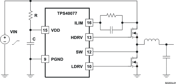
The regulator that supplies power for the drivers on the TPS40077 requires a limited rising slew rate on VDD for proper operation if the input voltage is above 10 V. If the slew rate is too great, this regulator can overshoot and damage to the part can occur. To ensure that the part operates properly, limit the slew rate to no more than 0.12 V/μs as the voltage at VDD crosses 8 V. If necessary, an R-C filter can be used on the VDD pin of the device. Connect the resistor from the VDD pin to the input supply of the converter. Connect the capacitor from the VDD pin to PGND. There should not be excessive (more than a 200-mV) voltage drop across the resistor in normal operation. This places some constraints on the R-C values that can be used. Figure 22 is a schematic fragment that shows the connection of the R-C slew rate limit circuit. Equation 1 and Equation 2 give values for R and C that limit the slew rate in the worst-case condition.
 Figure 22. Limiting the Slew Rate

where
- VVIN is the final value of the input voltage ramp
- fSW is the switching frequency
- Qg(TOT) is the combined total gate charge for both upper and lower MOSFETs (from MOSFET data sheet)
- IDD is the TPS40077 input current (3.5 mA maximum)
- SR is the maximum allowed slew rate [12 ×104] (V/s)