JAJSBU0F July 2012 – November 2020 TPS54020
PRODUCTION DATA
- 1 特長
- 2 アプリケーション
- 3 概要
- 4 Revision History
- 5 Description (Continued)
- 6 Pin Configuration and Functions
- 7 Specifications
-
8 Detailed Description
- 8.1 Overview
- 8.2 Functional Block Diagram
- 8.3
Feature Description
- 8.3.1 Fixed Frequency PWM Control
- 8.3.2 Input Voltage and Power Input Voltage Pins (VIN and PVIN)
- 8.3.3 Voltage Reference (VREF)
- 8.3.4 Adjusting the Output Voltage
- 8.3.5 Safe Start-up into Prebiased Outputs
- 8.3.6 Error Amplifier
- 8.3.7 Slope Compensation
- 8.3.8 Enable and Adjusting Undervoltage Lockout
- 8.3.9 Adjustable Switching Frequency and Synchronization (RT/CLK)
- 8.3.10 Soft-Start (SS) Sequence
- 8.3.11 Power Good (PWRGD)
- 8.3.12 Bootstrap Voltage (BOOT) and Low Dropout Operation
- 8.3.13 Sequencing (SS)
- 8.3.14 Output Overvoltage Protection (OVP)
- 8.3.15 Overcurrent Protection
- 8.3.16 Thermal Shutdown
- 8.4 Device Functional Modes
-
9 Application and Implementation
- 9.1 Application Information
- 9.2
Typical Application
- 9.2.1 Design Requirements
- 9.2.2
Detailed Design Procedure
- 9.2.2.1 Custom Design With WEBENCH® Tools
- 9.2.2.2 Operating Frequency
- 9.2.2.3 Output Inductor Selection
- 9.2.2.4 Output Capacitor Selection
- 9.2.2.5 Input Capacitor Selection
- 9.2.2.6 Soft-Start Capacitor Selection
- 9.2.2.7 Bootstrap Capacitor Selection
- 9.2.2.8 Undervoltage Lockout Set Point
- 9.2.2.9 Output Voltage Feedback Resistor Selection
- 9.2.2.10 Compensation Component Selection
- 9.2.3 Application Curves
- 10Power Supply Recommendations
- 11Layout
- 12Device and Documentation Support
- 13Mechanical, Packaging, and Orderable Information
パッケージ・オプション
メカニカル・データ(パッケージ|ピン)
- RUW|15
サーマルパッド・メカニカル・データ
- RUW|15
発注情報
8.3.13 Sequencing (SS)
Many of the common power supply sequencing methods can be implemented using the SS, EN, and PWRGD pins. The sequential method is illustrated in Figure 8-4 using two TPS54020 devices. The power good of the first device is coupled to the EN pin of the second device which enables the second power supply once the primary supply reaches regulation.
Figure 8-5 shows the method of implementing ratio-metric sequencing by connecting the SS pins of the two devices together. The regulator outputs ramp up and reach regulation at the same time. When calculating the soft-start time, the pullup current source must be doubled in Equation 4.

 Figure 8-5 Ratiometric Start-up
Sequence
Figure 8-5 Ratiometric Start-up
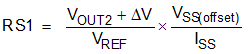
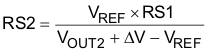
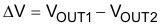
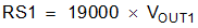
SequenceRatio-metric and simultaneous power supply sequencing can be implemented by connecting the resistor network of RS1 and RS2 shown in Figure 8-6 to the output of the power supply to which to be tracked, or alternately another voltage reference source. Using Equation 5 and Equation 6, the tracking resistors can be calculated to initiate the VOUT2 slightly before, after, or at the same time as VOUT1. Equation 7 is the voltage difference between VOUT1 and VOUT2. To design a ratio-metric start-up where the VOUT2 voltage is slightly greater than the VOUT1 voltage when VOUT2 reaches regulation, use a negative number in Equation 5 and Equation 6 for ΔV. Equation 7 results in a positive number for applications where VOUT2 is slightly lower than VOUT1 when VOUT2 regulation is achieved. The ΔV variable is zero volts for simultaneous sequencing. To minimize the effect of the inherent SS to VSENSE offset (VSS(offset), 29 mV) in the soft-start circuit and the offset created by the pullup current source (ISS, 2.3 μA) and tracking resistors, VSS(offset) and ISS are included as variables in the equations. To ensure start-up of VOUT2 after a fault, the calculated RS1 value from Equation 5 must be greater than the value calculated in Equation 8.
There are two important considerations when using a resistor divider to the SS/TR pin for simultaneous start-up. First, as described in Section 8.3.11, for the PWRGD output to be active, the SS/TR voltage must be above 1.4 V max. The external divider can prevent the SS/TR voltage from charging above the threshold. For the SS/TR pin to charge above the threshold, a switch can be needed to disconnect the resistor divider or modify the resistor divider ratio of the VOUT2 converter after start-up is complete. The PWRGD pin of the VOUT1 converter can be used for this. One solution is to add a resistor from SS/TR of the VOUT2 converter to the PWRGD of the VOUT1 converter. While the PWRGD of VOUT1 pulls low, this resistor will be in parallel with RS2. When VOUT1 is in regulation its PWRGD pin will float. If the PWRGD pin of VOUT1 is connected to a pullup voltage, make sure to include this in calculations. A second option is to use the PWRGD pin to turn on or turn off the external switch to change the divide ratio. The second consideration is that a pre-bias on VOUT1 can prevent VOUT2 from turning on. When the TPS54020 is enabled, an internal 500-Ω switch at the SS/TR pin turns on to discharge the SS/TR voltage as described in Section 8.3.10. The SS/TR pin voltage must discharge below 26 mV before the TPS54020 starts up. If the upper resistor at the SS/TR pin is too small, the SS/TR pin does not discharge below the threshold, and VOUT2 does not ramp up. The upper resistor in the SS/TR divider may need to be increased to allow the SS/TR pin to discharge below the threshold.
 Figure 8-6 Ratiometric and
Simultaneous Start-up Sequence
Figure 8-6 Ratiometric and
Simultaneous Start-up Sequence