JAJSDE0A June 2017 – February 2024 TPS549B22
PRODUCTION DATA
- 1
- 1 特長
- 2 アプリケーション
- 3 概要
- 4 Pin Configuration and Functions
- 5 Specifications
-
6 Detailed Description
- 6.1 Overview
- 6.2 Functional Block Diagram
- 6.3 Feature Description
- 6.4 Device Functional Modes
- 6.5 Programming
-
7 Register Maps
- 7.1 OPERATION Register (address = 1h)
- 7.2 ON_OFF_CONFIG Register (address = 2h)
- 7.3 CLEAR FAULTS (address = 3h)
- 7.4 WRITE PROTECT (address = 10h)
- 7.5 STORE_DEFAULT_ALL (address = 11h)
- 7.6 RESTORE_DEFAULT_ALL (address = 12h)
- 7.7 CAPABILITY (address = 19h)
- 7.8 VOUT_MODE (address = 20h)
- 7.9 VOUT_COMMAND (address = 21h)
- 7.10 VOUT_MARGIN_HIGH (address = 25h) ®
- 7.11 VOUT_MARGIN_LOW (address = 26h)
- 7.12 STATUS_BYTE (address = 78h)
- 7.13 STATUS_WORD (High Byte) (address = 79h)
- 7.14 STATUS_VOUT (address = 7Ah)
- 7.15 STATUS_IOUT (address = 7Bh)
- 7.16 STATUS_CML (address = 7Eh)
- 7.17 MFR_SPECIFIC_00 (address = D0h)
- 7.18 MFR_SPECIFIC_01 (address = D1h)
- 7.19 MFR_SPECIFIC_02 (address = D2h)
- 7.20 MFR_SPECIFIC_03 (address = D3h)
- 7.21 MFR_SPECIFIC_04 (address = D4h)
- 7.22 MFR_SPECIFIC_06 (address = D6h)
- 7.23 MFR_SPECIFIC_07 (address = D7h)
- 7.24 MFR_SPECIFIC_44 (address = FCh)
-
8 Application and Implementation
- 8.1 Application Information
- 8.2
Typical Applications
- 8.2.1 TPS549B22 1.5-V to 18-V Input, 1-V Output, 25-A Converter
- 8.2.2 Design Requirements
- 8.2.3
Detailed Design Procedure
- 8.2.3.1 Custom Design With WEBENCH® Tools
- 8.2.3.2 Switching Frequency Selection
- 8.2.3.3 Inductor Selection
- 8.2.3.4 Output Capacitor Selection
- 8.2.3.5 Input Capacitor Selection
- 8.2.3.6 Bootstrap Capacitor Selection
- 8.2.3.7 BP Pin
- 8.2.3.8 R-C Snubber and VIN Pin High-Frequency Bypass
- 8.2.3.9 Optimize Reference Voltage (VSEL)
- 8.2.3.10 MODE Pin Selection
- 8.2.3.11 ADDR Pin Selection
- 8.2.3.12 Overcurrent Limit Design
- 8.2.4 Application Curves
- 8.3 Power Supply Recommendations
- 8.4 Layout
- 9 Device and Documentation Support
- 10Revision History
- 11Mechanical, Packaging, and Orderable Information
パッケージ・オプション
デバイスごとのパッケージ図は、PDF版データシートをご参照ください。
メカニカル・データ(パッケージ|ピン)
- RVF|40
サーマルパッド・メカニカル・データ
- RVF|40
発注情報
8.2.3.4.2 Response to a Load Transient
The output capacitance must supply the load with the required current when current is not immediately provided by the regulator. When the output capacitor supplies load current, the impedance of the capacitor greatly affects the magnitude of voltage deviation (such as undershoot and overshoot) during the transient.
Use Equation 8 and Equation 9 to estimate the amount of capacitance needed for a given dynamic load step and release.
There are other factors that can impact the amount of output capacitance for a specific design, such as ripple and stability.
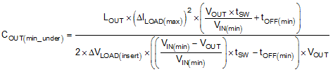
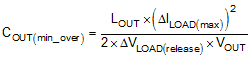
where
- COUT(min_under) is the minimum output capacitance to meet the undershoot requirement
- COUT(min_over)is the minimum output capacitance to meet the overshoot requirement
- L is the output inductance value (0.33 µH)
- ∆ILOAD(max) is the maximum transient step (15 A)
- VOUT is the output voltage value (1 V)
- tSW is the switching period (1.54 µs)
- VIN(min) is the minimum input voltage for the design (10.8 V)
- tOFF(min) is the minimum off time of the device (300 ns)
- ∆VLOAD(insert) is the undershoot requirement (30 mV)
- ∆VLOAD(release) is the overshoot requirement (30 mV)
Most of the above parameters can be found in Table 8-1.
The minimum output capacitance to meet the undershoot requirement is 516 µF. The minimum output capacitance to meet the overshoot requirement is 1238 µF. This example uses a combination of POSCAP and MLCC capacitors to meet the overshoot requirement.
- POSCAP bank 1: 2 x 470 µF, 2.5 V, 6 mΩ per capacitor
- MLCC bank 2: 7 × 100 µF, 2.5 V, 1 mΩ per capacitor with DC+AC derating factor of 60%
Recalculating the worst case overshoot using the described capacitor bank design, the overshoot is 29.0 mV which meets the 30-mV overshoot specification requirement.