SLVS952G April   2010  – January 2017 TPS62671 , TPS62672 , TPS62674 , TPS62675 , TPS626751 , TPS626765 , TPS62679

PRODUCTION DATA.  

  1. Features
  2. Applications
  3. Description
  4. Simplified Schematic
  5. Revision History
  6. Device Comparison Table
  7. Pin Configuration and Functions
  8. Specifications
    1. 8.1 Absolute Maximum Ratings
    2. 8.2 Handling Ratings
    3. 8.3 Recommended Operating Conditions
    4. 8.4 Thermal Information
    5. 8.5 Electrical Characteristics
    6. 8.6 Typical Characteristics
  9. Parameter Measurement Information
  10. 10Detailed Description
    1. 10.1 Overview
    2. 10.2 Functional Block Diagram
    3. 10.3 Feature Description
      1. 10.3.1 Switching Frequency
      2. 10.3.2 Power Save Mode
      3. 10.3.3 Mode Selection
      4. 10.3.4 Spread Spectrum, PWM Frequency Dithering
      5. 10.3.5 Short-Circuit Protection
      6. 10.3.6 Thermal Shutdown
    4. 10.4 Device Functional Modes
      1. 10.4.1 Soft Start
      2. 10.4.2 Enable
      3. 10.4.3 Active Output Discharge
      4. 10.4.4 Undervoltage Lockout
  11. 11Application and Implementation
    1. 11.1 Application Information
    2. 11.2 Typical Applications
      1. 11.2.1 TPS6267x Point-Of-Load Supply
        1. 11.2.1.1 Design Requirements
        2. 11.2.1.2 Detailed Design Procedure
          1. 11.2.1.2.1 Inductor Selection
          2. 11.2.1.2.2 Output Capacitor Selection
          3. 11.2.1.2.3 Input Capacitor Selection
          4. 11.2.1.2.4 Checking Loop Stability
        3. 11.2.1.3 Application Curves
      2. 11.2.2 1.26V CMOS Sensor Embedded Power Solution — Featuring Sub 0.4mm Profile
        1. 11.2.2.1 Design Requirements
        2. 11.2.2.2 Detailed Design Procedure
        3. 11.2.2.3 Application Curves
  12. 12Power Supply Recommendations
  13. 13Layout
    1. 13.1 Layout Guidelines
    2. 13.2 Layout Example
  14. 14Device and Documentation Support
    1. 14.1 Device Support
      1. 14.1.1 Third-Party Products Disclaimer
    2. 14.2 Documentation Support
      1. 14.2.1 Related Documentation
        1. 14.2.1.1 References
    3. 14.3 Related Links
    4. 14.4 Trademarks
    5. 14.5 Electrostatic Discharge Caution
    6. 14.6 Glossary
  15. 15Mechanical, Packaging, and Orderable Information

パッケージ・オプション

メカニカル・データ(パッケージ|ピン)
サーマルパッド・メカニカル・データ
発注情報

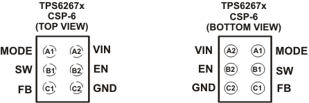
Pin Configuration and Functions

TPS62671 TPS62672 TPS62674 TPS62675 TPS626751 TPS626765 TPS62679 po_6267_lvs952.gif

Pin Functions

PIN I/O DESCRIPTION
NAME NO.
FB C1 I Output feedback sense input. Connect FB to the converter’s output.
VIN A2 I Power supply input.
SW B1 I/O This is the switch pin of the converter and is connected to the drain of the internal Power MOSFETs.
EN B2 I This is the enable pin of the device. Connecting this pin to ground forces the device into shutdown mode. Pulling this pin to VI enables the device. If an external clock (4MHz to 27MHz) is detected the device will automatically power up. This pin must not be left floating and must be terminated.
MODE A1 I This is the mode selection pin of the device. This pin must not be left floating and must be terminated.
MODE = LOW: The device is operating in regulated frequency pulse width modulation mode (PWM) at high-load currents and in pulse frequency modulation mode (PFM) at light load currents.
MODE = HIGH: Low-noise mode enabled, regulated frequency PWM operation forced.
GND C2 Ground pin.